Surface flatness measurement is a critical process in optical manufacturing, ensuring the precision and performance of lenses, mirrors, and other optical components. This intricate process typically involves *interferometry*, a highly accurate method that utilizes light waves to detect minute deviations from a perfectly flat surface, often down to a fraction of a wavelength. By ensuring unparalleled accuracy, optical manufacturers can guarantee the superior quality and functionality of their products, from high-power lasers to medical imaging systems.
Understanding the Imperative: Why is Surface Flatness So Crucial in Optics?
In the realm of optical manufacturing, the flatness of a surface is not merely a desirable quality; it is a fundamental requirement that underpins the entire performance of an optical system. Any deviation from perfect flatness, even at the sub-nanometer scale, can introduce aberrations, distort wavefronts, and significantly degrade the quality of light transmitted or reflected. For applications ranging from astronomical telescopes that demand picometer precision to advanced lithography systems critical for semiconductor manufacturing, the integrity of the optical wavefront is paramount. Imperfect flatness can lead to a phenomenon known as wavefront error, where the intended path of light is subtly altered, resulting in blurred images, reduced resolution, and decreased efficiency of light transmission. This is particularly evident in high-power laser optics, where even a slight surface imperfection can cause scattering, energy loss, and even catastrophic damage due to localized heat absorption. Therefore, understanding and meticulously controlling surface flatness is not just about meeting specifications; it’s about enabling the advanced capabilities that define modern optical technology.
The impact of surface flatness extends beyond mere image quality. In applications like interferometers themselves, which rely on the precise interference of light waves, the flatness of reference surfaces directly dictates the accuracy and reliability of the measurements. Similarly, in thin-film coatings, the substrate’s flatness influences the uniformity and adhesion of deposited layers, affecting spectral performance and durability. Without rigorous flatness control, the theoretical performance of an optical design often remains an elusive ideal. The ability to precisely quantify and correct these minute surface deviations is what distinguishes high-performance optical components from their less precise counterparts, directly contributing to the success of scientific research, industrial innovation, and critical defense applications. This foundational requirement necessitates sophisticated measurement techniques capable of resolving features far smaller than the human eye can perceive, pushing the boundaries of metrology.
Defining Surface Flatness: Key Parameters and Specifications
When discussing surface flatness in optical manufacturing, it’s essential to understand the specific parameters used to quantify this critical characteristic. Flatness is generally defined as the deviation of a surface from a true geometric plane. The most common metrics used are often expressed in terms of wavelengths (λ) of light, typically the helium-neon laser’s wavelength of 632.8 nm, or in fractions of an inch or millimeters. A common specification might be “λ/10” (one-tenth of a wavelength), indicating a very high degree of flatness. This specification refers to the peak-to-valley (PV) deviation, which is the maximum difference in height between the highest and lowest points on the measured surface relative to a reference plane. A smaller PV value signifies a flatter surface. Another crucial parameter is the Root Mean Square (RMS) deviation, which provides a statistical measure of the average deviation of the surface from the ideal plane. While PV gives an indication of the extreme variations, RMS offers a more comprehensive view of the overall surface quality, as it is less sensitive to isolated peaks or valleys. Optical engineers often use both PV and RMS values to fully characterize a surface, with RMS being particularly useful for predicting the scattering and wavefront error performance of a component. Understanding these parameters is foundational to both specifying and verifying the quality of optical surfaces.
Beyond PV and RMS, other specifications like irregularity and power are also used. Irregularity refers to the local deviations from the ideal spherical or plano shape after the overall curvature (power) has been removed. Power describes the overall curvature of the surface, essentially how much the surface deviates from a flat plane or ideal sphere, much like the “power” of a lens. A perfectly flat surface would have zero power. These parameters are often measured simultaneously using advanced interferometric techniques and are critical for ensuring that an optical component performs as designed within a larger optical system. For instance, a mirror might be specified as having λ/20 flatness with λ/50 irregularity, indicating a very flat surface with minimal localized imperfections. The choice of specification depends heavily on the intended application and the required optical performance. High-precision applications, such as those in scientific instrumentation or advanced lithography, demand extremely tight flatness tolerances, often in the range of λ/20 to λ/100, while less demanding applications might tolerate λ/4 or λ/2 specifications. The ability to measure and control these intricate parameters is a hallmark of high-quality optical manufacturing.
Unveiling the Techniques: How Do We Precisely Measure Flatness?
The precision required for optical flatness measurement necessitates highly sophisticated techniques, with interferometry standing as the gold standard. These methods exploit the wave nature of light to detect minute surface variations that are imperceptible to the naked eye or even high-magnification microscopes. The fundamental principle behind interferometry involves combining two beams of light: one reference beam from a perfectly flat reference surface and another measurement beam reflected from the test surface. When these two beams recombine, they create an interference pattern of bright and dark fringes. These fringes are essentially a contour map of the test surface, where each fringe represents a height difference equivalent to half a wavelength of light. By analyzing the shape, number, and distribution of these fringes, engineers can accurately determine the flatness, or lack thereof, of the optical component. This non-contact measurement method offers exceptional accuracy, often achieving resolutions down to fractions of a nanometer, which is indispensable for modern optical fabrication.
While traditional interferometers provide invaluable data, advancements have led to the development of several specialized interferometric techniques tailored for different applications and levels of precision. These techniques often incorporate sophisticated software algorithms for fringe analysis and environmental controls to ensure accuracy. The choice of method depends on factors such as the size and shape of the optical component, the required measurement accuracy, the cost constraints, and the specific defects being investigated. Each technique offers a unique advantage, allowing optical manufacturers to select the most appropriate tool for their specific metrology challenges. The continuous evolution of these measurement systems reflects the increasing demands for precision and quality in the rapidly advancing field of optics.
Optical Flats & Monochromatic Light: The Foundation of Comparison
Before the advent of sophisticated digital interferometers, and still widely used for quick, qualitative assessments, *optical flats* paired with monochromatic light formed the cornerstone of surface flatness measurement. An optical flat is a highly polished, precisely manufactured piece of glass or fused silica with one or both surfaces ground and polished to an extremely high degree of flatness (often λ/20 or better). When the test surface is placed in close proximity to a reference optical flat, and monochromatic light (light of a single wavelength, typically from a sodium or helium lamp) is shone upon them, a phenomenon called Newton’s Rings or interference fringes becomes visible. The thin air gap between the two surfaces acts as an interferometer. Light waves reflecting from the bottom of the optical flat and the top of the test surface interfere with each other. Where the path difference between these two reflected waves is an integer multiple of the wavelength, constructive interference occurs, creating bright fringes. Where the path difference is a half-integer multiple, destructive interference occurs, resulting in dark fringes. These fringes form a contour map, with each fringe representing a contour line of constant height separation, typically half a wavelength.
By observing the pattern of these interference fringes, a skilled optician can quickly assess the flatness of the test surface. Perfectly straight, parallel, and evenly spaced fringes indicate an excellent flat surface. Curved or irregularly spaced fringes reveal deviations such as convexity, concavity, astigmatism, or localized defects. The number of fringes provides a quantitative estimate of the overall wedge or tilt between the two surfaces, while their curvature directly relates to the flatness deviation. For example, a perfectly flat surface with a slight wedge between it and the optical flat will produce straight, evenly spaced parallel lines. If the surface is concave, the fringes will bow towards the point of contact; if convex, they will bow away. While this method is highly effective for visual inspection and relatively rapid assessment, it is often qualitative or semi-quantitative. It requires a skilled operator to interpret the patterns and typically doesn’t provide the precise numerical data (like PV or RMS) that modern digital interferometers offer, yet it remains an invaluable tool for preliminary quality control and in situations where complex equipment is not available or necessary.
Phase-Shifting Interferometry (PSI): The Digital Revolution
Phase-Shifting Interferometry (PSI) represents a significant leap forward in optical flatness measurement, transforming it from a qualitative visual assessment to a highly precise, quantitative digital process. Unlike traditional interferometry that relies on static fringe patterns, PSI introduces a controlled phase shift between the reference and test beams over multiple measurements. This is typically achieved by precisely moving the reference mirror with a piezoelectric transducer (PZT) through a fraction of a wavelength, or by modulating the wavelength of the light source. At each step of the phase shift (e.g., 0, 90, 180, and 270 degrees), a digital camera captures the resulting interference pattern. These multiple images, each with a different phase relationship, contain redundant information about the surface topography. Advanced algorithms then mathematically process these captured intensity maps to extract the precise phase difference at each pixel across the entire surface. This phase difference directly corresponds to the height variation of the test surface relative to the reference, allowing for the creation of a high-resolution 3D topographical map.
The key advantage of PSI lies in its ability to extract a precise phase map, which is insensitive to intensity variations across the beam and provides much higher resolution and accuracy than traditional fringe analysis. By removing ambiguities associated with fringe interpretation, PSI can resolve surface features down to nanometers or even sub-nanometer levels, offering quantitative data on PV, RMS, and various Zernike polynomial coefficients that describe specific types of aberrations (e.g., tilt, defocus, astigmatism, coma). This digital output is not only precise but also repeatable, enabling automated quality control and detailed statistical process analysis in manufacturing. PSI systems are widely adopted in critical applications such such as semiconductor lithography, high-power laser optics, and precision optical metrology, where the exact quantitative characterization of surface form error is paramount. Its capability to provide a full-field map of the surface significantly enhances the understanding and control over the manufacturing process, making it an indispensable tool for achieving the most stringent flatness requirements.
Fizeau Interferometers: The Workhorse of Optical Metrology
The *Fizeau interferometer* is arguably the most prevalent and versatile instrument used for surface flatness measurement in optical manufacturing, especially for plano (flat) surfaces and spherical components. Its robust design and high accuracy make it the workhorse of optical metrology labs worldwide. At its core, a Fizeau interferometer operates by directing a collimated beam of coherent light, typically from a laser, towards a high-quality reference flat (or a reference sphere for curved surfaces). A small portion of the incident light reflects directly from the reference surface, forming the reference beam. The remaining light passes through the reference surface and reflects off the test surface. This reflected light then travels back through the reference surface, where it recombines with the reference beam. Because the reference and test surfaces are placed in close proximity, the two reflected beams are nearly collinear, minimizing angular errors and making the system robust against vibration. The combined beams then interfere, and the resulting fringe pattern is captured by a camera. Modern Fizeau interferometers often incorporate Phase-Shifting Interferometry (PSI) techniques to precisely quantify the surface topography.
What sets the Fizeau design apart is its common path configuration for the reference and test beams, meaning they travel very similar optical paths. This design inherently reduces sensitivity to environmental disturbances like air turbulence and vibration, leading to highly stable and repeatable measurements. Furthermore, Fizeau interferometers are capable of measuring a wide range of surface sizes and materials, from small optical components to large telescope mirrors. They can be configured with various transmission spheres (precisely manufactured lenses that produce a converging or diverging wavefront) to measure concave or convex spherical surfaces in addition to flats. The sophisticated software accompanying these systems allows for detailed analysis of the measured surface data, providing comprehensive reports including PV, RMS, wavefront error maps, and Zernike polynomial decompositions. This detailed characterization is essential for identifying specific manufacturing errors and guiding the polishing process. The Fizeau interferometer’s combination of precision, versatility, and reliability has cemented its status as an indispensable tool for ensuring the highest quality of optical surfaces in a multitude of applications, from medical devices to aerospace optics.
Twyman-Green Interferometers: Versatility for Complex Shapes
While the Fizeau interferometer excels at measuring plano and spherical surfaces, the *Twyman-Green interferometer* offers greater versatility, particularly for assessing the wavefront quality of complex optical components like prisms, lenses, and assemblies, as well as highly challenging surfaces that might be difficult to measure with a Fizeau. Derived from the classic Michelson interferometer, the Twyman-Green design utilizes a beam splitter to divide a single coherent light beam into two distinct paths: a reference arm and a test arm. The reference arm typically contains a high-quality reference mirror, providing a flat wavefront. The test arm contains the optical component being evaluated. After reflecting off their respective elements, the two beams are recombined by the beam splitter, and the resulting interference pattern is captured by a detector. Unlike the common-path Fizeau, the Twyman-Green’s separated paths allow for independent manipulation and optimization of each arm, providing flexibility for measuring transmitted wavefronts through optical elements or highly divergent wavefronts from objective lenses.
The primary advantage of the Twyman-Green configuration is its adaptability. By placing different optical components in the test arm, it can be used to measure not only surface flatness (by reflecting off the surface) but also the transmitted wavefront error of lenses and prisms, or the overall wavefront quality of entire optical systems. For example, a lens can be placed in the test arm, and its transmitted wavefront can be compared to a perfect reference wavefront, revealing aberrations introduced by the lens itself. This makes it an invaluable tool for validating the performance of assembled optics. However, the separated paths also make Twyman-Green interferometers more sensitive to environmental factors like vibration and air turbulence compared to Fizeau designs, often requiring more stringent environmental control for high-precision measurements. Despite this, its capability to provide detailed wavefront analysis for a broad spectrum of optical components ensures its continued importance in advanced optical metrology, particularly where system-level performance verification is critical.
Profilometers: Direct Surface Topography Mapping
Beyond interferometric methods, *profilometers* offer another class of instruments for directly mapping surface topography, including flatness. Unlike interferometers that measure deviations from a wavefront, profilometers physically or optically scan the surface point by point or line by line to build a direct height profile. There are two primary types: contact profilometers and non-contact profilometers. *Contact profilometers*, also known as stylus profilometers, use a very fine diamond-tipped stylus that is dragged across the surface. As the stylus traverses the surface, its vertical displacement is precisely measured, generating a 2D profile of the surface roughness and form. While highly accurate for measuring surface roughness parameters, the physical contact can potentially scratch or damage delicate optical surfaces, making them less ideal for finished optics. However, they are often used for measuring the form of molds, substrates, or rougher surfaces prior to final polishing.
*Non-contact profilometers*, on the other hand, utilize optical principles to achieve their measurements, thus avoiding any risk of damage to the surface. These include:
- Optical Profilometers (White Light Interferometers): These instruments use broad-spectrum (white) light and interferometric principles to measure surface height. By scanning the focus vertically or by using chromatic aberration, they can determine the height at each point, creating a 3D topographical map. They are excellent for measuring surface roughness and form on polished optical surfaces, often providing sub-nanometer vertical resolution.
- Confocal Microscopes: These use a spatial pinhole at the conjugate focal plane of the objective lens to block out-of-focus light, allowing for optical sectioning and the creation of 3D images. By scanning vertically, they can build a detailed topographical map of a surface. They are particularly useful for measuring rough surfaces or features with steep slopes.
- Atomic Force Microscopes (AFM): While typically used for nanometer-scale surface roughness rather than overall flatness of large areas, AFMs can provide incredibly high-resolution 3D topography. A sharp tip attached to a cantilever scans the surface, and interatomic forces cause the cantilever to deflect. These deflections are measured to create a topographical map. AFMs are primarily used for research and characterization of very small areas or critical defects.
Non-contact profilometers are valuable for their ability to measure a wide range of surface textures and features without damage, complementing interferometric measurements by providing detailed local information about roughness and microscopic defects that might not be fully resolved by larger-field interferometers. They are particularly useful for micro-optics and surfaces with complex features.
The Measurement Process: From Setup to Interpretation
The journey of precisely measuring surface flatness in optical manufacturing is a meticulous process that extends far beyond simply placing a component in an instrument. It encompasses a series of critical steps, from the initial preparation of the measurement environment and the optical component itself, through the careful execution of the measurement, to the sophisticated analysis and interpretation of the acquired data. Each stage plays a vital role in ensuring the accuracy, reliability, and validity of the flatness assessment. Adhering to best practices at every step is crucial, as even minor oversights can introduce errors that compromise the integrity of the measurement. This holistic approach ensures that the final flatness specifications truly reflect the quality of the optical surface, guiding both manufacturing adjustments and final product acceptance. The entire process is a testament to the interplay of advanced metrology equipment, skilled technicians, and robust analytical tools, all aimed at achieving unparalleled optical precision.
Environmental Controls: Minimizing External Influences
Achieving highly accurate surface flatness measurements in optical manufacturing demands rigorous control over the measurement environment. Even minute external influences can significantly degrade the precision of interferometric systems, where measurements are often conducted down to nanometer or sub-nanometer scales. The three primary environmental factors that require strict regulation are temperature, vibration, and air quality. *Temperature stability* is paramount because optical materials expand and contract with temperature changes. A change of just a few degrees Celsius can cause an optical component to deform, introducing apparent flatness errors that are not inherent to the surface itself. Therefore, measurement labs are typically maintained within a very tight temperature range (e.g., ±0.1°C or even ±0.01°C) with minimal gradients across the measurement area. This often involves HVAC systems with precise temperature control and isolation from external heat sources.
*Vibration isolation* is equally critical. Ground vibrations from nearby machinery, foot traffic, or even distant road traffic can cause relative motion between the interferometer’s components and the test part during measurement. Since interferometers detect displacements smaller than the wavelength of light, even microscopic vibrations can blur fringe patterns or introduce measurement noise. High-precision interferometers are typically mounted on active or passive vibration isolation tables, which use pneumatic systems, springs, or electronic feedback mechanisms to damp out vibrations. Lastly, *air quality control* plays a crucial role. Dust particles can settle on optical surfaces, creating false high points or scattering light. Air turbulence, caused by convection currents or air conditioning drafts, introduces refractive index variations that distort the wavefront of light, leading to erroneous measurements. Cleanroom environments (e.g., Class 100 or Class 1000) with laminar airflow systems are often employed to minimize dust and maintain stable air conditions. By meticulously controlling these environmental parameters, manufacturers can ensure that the measured flatness truly represents the optical component’s intrinsic surface quality, rather than artifacts introduced by the surroundings.
Sample Preparation and Handling: Preserving Integrity
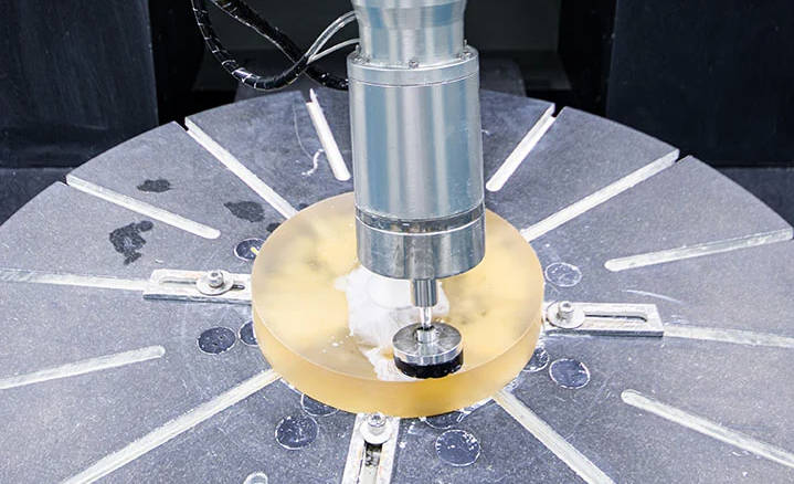
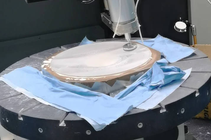
The integrity of surface flatness measurements hinges not only on advanced instrumentation and environmental controls but also critically on the meticulous *preparation and handling of the optical sample itself*. Any contamination or damage to the optical surface before or during measurement can irrevocably compromise the accuracy of the results. The first step in sample preparation is thorough cleaning. Optical surfaces must be free from dust, fingerprints, oils, residues, and any other particulate matter that could interfere with light reflection or adhesion to the measurement chuck. This typically involves a multi-step cleaning process, often starting with gentle swabbing with optical-grade solvents (e.g., isopropyl alcohol, acetone) and lint-free wipes, followed by ultrasonic cleaning in specialized solutions, and a final rinse with deionized water. Air drying with filtered nitrogen or an ionization gun is then used to prevent water spots and static charge build-up. The goal is a pristine, film-free surface that accurately represents its true topography.
Once clean, careful handling is paramount. Optical components should only be touched on their edges, preferably with clean, lint-free gloves, to prevent transferring oils or residues from skin. During measurement, the optical component must be properly mounted and supported to prevent mechanical stress or deformation, which can introduce apparent flatness errors. For instance, thin optics can sag under their own weight if not properly supported, leading to misleading “concave” measurements. Special care is taken to use appropriate fixturing that holds the part securely without distorting its shape. Additionally, allowing the sample to *thermally equilibrate* within the controlled measurement environment for a sufficient period (often several hours) before measurement is crucial. This prevents thermal gradients within the optic itself from causing temporary deformations that would affect the flatness reading. By adhering to these stringent protocols for sample preparation and handling, optical manufacturers ensure that the measured data truly reflects the intrinsic flatness of the component, rather than artifacts introduced by improper treatment.
Data Acquisition & Analysis: Unveiling Surface Topography
Once the optical component is prepared and positioned within the controlled environment of an interferometer, the *data acquisition and analysis* phase begins, transforming raw optical interference patterns into quantitative insights about surface flatness. In modern interferometry, particularly with Phase-Shifting Interferometers (PSI) and Fizeau systems, this process is largely automated and driven by sophisticated software. During data acquisition, the interferometer captures a series of digital images of the interference fringes as the phase between the reference and test beams is systematically varied. For PSI, typically 3 to 10 images are captured, each with a precisely known phase shift. These images are then fed into the system’s software.
The analysis software then employs complex algorithms to process these raw intensity maps. The primary goal is to *unwrap the phase* from the captured intensity patterns, effectively converting the grayscale fringe data into a precise, continuous phase map across the entire measured surface. This phase map directly corresponds to the height variations of the test surface relative to the reference. Once the phase map is generated, the software proceeds to calculate various key flatness parameters:
- Peak-to-Valley (PV) Deviation: The absolute difference between the highest and lowest points on the measured surface, typically expressed in wavelengths (λ) or nanometers.
- Root Mean Square (RMS) Deviation: A statistical measure of the average deviation of the surface from the ideal plane, providing a more comprehensive indication of overall surface quality.
- Zernike Polynomial Coefficients: These mathematical polynomials are used to decompose the surface topography into specific aberration types (e.g., tilt, defocus, astigmatism, coma, spherical aberration). This decomposition is invaluable for diagnosing the root cause of manufacturing errors, as certain Zernike terms are often indicative of specific polishing or grinding issues.
- 3D Topographical Maps: The software generates visual representations, often color-coded, that graphically depict the surface height variations, making it easy to identify high points, low points, and localized defects.
- Line Profiles and Cross-Sections: Users can extract 2D profiles along specific lines across the surface to examine localized features in detail.
The output reports are comprehensive, often including numerical values for all relevant parameters, graphical plots, and statistical analysis. This detailed quantitative data is critical for quality control, process improvement, and certifying the optical component meets its stringent design specifications, ensuring its optimal performance within the final optical system.
Beyond the Basics: Advanced Considerations & Challenges
While the fundamental principles and established techniques for surface flatness measurement are well-defined, the relentless pursuit of optical perfection in cutting-edge applications introduces a layer of complexity that goes “beyond the basics.” Advanced optical manufacturing often involves components with extreme specifications, novel materials, or challenging geometries that push the limits of conventional metrology. These scenarios demand innovative approaches, a deep understanding of metrological limitations, and careful consideration of factors that might be less critical for standard optics. Addressing these advanced considerations and overcoming inherent challenges is paramount for supporting the next generation of optical technologies, from high-energy laser systems and gravitational wave detectors to advanced space telescopes and quantum computing components. It requires continuous research and development in metrology, along with a collaborative effort between optical designers, manufacturers, and metrology specialists to bridge the gap between theoretical precision and practical measurement capabilities.
Measuring Large Optics: Addressing Sag and Stitching
Measuring the flatness of *large optical components*, such as astronomical telescope mirrors (e.g., 8-meter primaries) or large lithography optics, presents unique and formidable challenges that extend beyond the capabilities of standard interferometers. One of the most significant issues is *gravitational sag*. Even perfectly manufactured large optics can deform under their own weight, especially when oriented horizontally for measurement. This sag can mimic a curvature, making an intrinsically flat surface appear concave or convex. To counteract this, sophisticated support systems are employed, often using pneumatic or hydraulic actuators to actively compensate for gravity and maintain the intended surface form during measurement. Furthermore, specialized algorithms are used to model and subtract the predictable sag from the measurement data, revealing the true intrinsic flatness.
Another major challenge for large optics is that their size often exceeds the field of view of even large-aperture interferometers. This necessitates a technique known as *stitching interferometry*. In this method, the large surface is divided into numerous smaller, overlapping sub-apertures. An interferometer then measures each sub-aperture individually. Sophisticated software algorithms then “stitch” these individual measurements together, using the overlap regions to precisely align and combine the data into a single, comprehensive topographical map of the entire surface. This stitching process requires incredibly accurate positioning systems for the interferometer head or the part itself, along with robust algorithms that can handle local errors and ensure continuity across the stitched boundaries. For very large, segmented mirrors, like those used in modern telescopes, each segment might be individually measured and then its performance verified as part of the overall assembly using dedicated alignment and phasing techniques. The combination of gravitational sag compensation and stitching interferometry allows for the precise characterization of exceptionally large optical surfaces, enabling the construction of cutting-edge astronomical instruments and other demanding large-scale optical systems.
Impact of Coatings: Thin Films and Their Influence
The vast majority of precision optical components are not used “bare”; they are covered with *thin-film coatings* designed to enhance their performance, such as anti-reflection (AR) coatings, high-reflection (HR) coatings, or spectral filters. While these coatings are critical for functionality, they can also subtly influence surface flatness measurements and introduce their own set of metrological challenges. Firstly, the thickness and uniformity of the coating itself can affect the perceived flatness. If a coating is not perfectly uniform, variations in its thickness can lead to apparent topographical changes, even if the underlying substrate is perfectly flat. This is particularly relevant for thick coatings or those with steep thickness gradients. Modern interferometers often measure the optical path difference, and variations in the refractive index or thickness of a coating can manifest as false height errors.
Secondly, the deposition process of thin films can induce *stress* in the optical substrate. Depending on the material, deposition parameters, and substrate properties, coatings can be either in tensile or compressive stress. This stress, if significant, can cause the substrate to bow or deform, directly impacting its flatness. For example, a highly stressed coating on a thin mirror can cause it to become slightly concave or convex, thereby changing its optical power. Measuring the flatness before and after coating deposition is often crucial to quantify this coating-induced deformation. Furthermore, the optical properties of the coating (reflectivity, transparency) at the measurement wavelength can affect the signal-to-noise ratio of the interferometer. Highly reflective coatings are generally easier to measure, while highly transmissive or absorbing coatings might require specialized techniques or careful adjustment of interferometer parameters to obtain a clear interference pattern. Therefore, when measuring coated optics, it is essential to consider the coating’s properties, potential stress effects, and its interaction with the measurement wavelength to accurately assess the true surface flatness and its overall impact on the component’s performance.
Traceability and Calibration: Ensuring Measurement Confidence
In the high-stakes world of optical manufacturing, where nanometer-level precision is commonplace, *traceability and calibration* are not just best practices; they are fundamental pillars that instill confidence in measurement results and ensure the reliability of optical components. *Traceability* means that a measurement result can be related to a national or international standard through an unbroken chain of comparisons, all with stated uncertainties. For surface flatness, this typically means that the interferometer used for measurement must itself be calibrated against a primary or secondary standard whose flatness is known with a very high degree of certainty and is traceable to recognized metrology institutes like NIST (National Institute of Standards and Technology) or PTB (Physikalisch-Technische Bundesanstalt).
*Calibration* involves systematically comparing the interferometer’s readings against known standards. For flatness, this often includes using certified reference flats or calibrated sphere standards. These reference artifacts have their flatness or radius of curvature characterized with extremely low uncertainty by a higher-level metrology lab. During calibration, the interferometer measures these known standards, and any observed deviations are used to adjust the instrument’s settings or to generate a correction map that can be applied to subsequent measurements of unknown parts. Regular calibration, performed at specified intervals (e.g., annually) or after significant events (e.g., instrument repair), is crucial to ensure that the interferometer maintains its accuracy over time. This also involves validating the instrument’s ability to measure common aberrations like astigmatism and spherical aberration using known test parts. Without proper traceability and regular calibration, flatness measurements, no matter how sophisticated the equipment, lack scientific and legal credibility. This commitment to metrological traceability ensures that when an optical component is specified to be “λ/20 flat,” that claim is underpinned by a robust, internationally recognized system of measurement standards, guaranteeing quality and performance across the global optical industry.
The Future of Flatness Metrology: Innovations on the Horizon
The field of surface flatness metrology is far from static; it is a dynamic area of research and development driven by the ever-increasing demands for precision in optical manufacturing. As new optical applications emerge—from extreme ultraviolet (EUV) lithography and high-power laser systems to advanced quantum technologies and adaptive optics—the need for faster, more accurate, and more versatile flatness measurement techniques continues to grow. These future innovations will likely focus on pushing the boundaries of spatial resolution, reducing measurement times, expanding the range of measurable surface types, and integrating metrology more seamlessly into automated production environments. The pursuit of optical perfection is an endless journey, and the tools we use to quantify it must continuously evolve to meet the challenges of tomorrow’s optical frontiers.
Non-Contact, High-Speed, and In-Situ Measurements
The future of flatness metrology is trending towards methods that are *non-contact*, *high-speed*, and capable of *in-situ measurements*, moving away from traditional, often time-consuming, and offline metrology. The shift towards non-contact techniques is driven by the desire to prevent any possibility of damage or contamination to delicate optical surfaces, especially as components become increasingly sophisticated and expensive. Technologies like advanced optical profilometers using white light interferometry, or even X-ray interferometry for subsurface analysis, will become more prevalent for their ability to provide comprehensive surface data without physical interaction.
*High-speed measurement* is becoming crucial for high-volume manufacturing and for enabling real-time process control. Current interferometric measurements can take minutes, which is too slow for some rapidly moving production lines. Future systems are being developed that can capture and process data almost instantaneously, potentially utilizing parallel processing techniques or novel optical architectures that capture full-field data in a single shot. This will allow for 100% inspection of components, rather than relying on statistical sampling. The ultimate goal is *in-situ measurement*, where flatness can be assessed directly within the manufacturing environment—for instance, during the polishing process, without removing the part from the machine. This would provide immediate feedback, allowing for active, real-time adjustments to the polishing tool path or parameters, dramatically improving efficiency and reducing scrap rates. Techniques like deflectometry, which measures surface slope variations, are showing promise for in-situ, non-contact measurements, particularly for freeform optics. Integrating these advanced metrology systems directly into automated manufacturing cells will revolutionize the production of precision optics, making the manufacturing process more agile, precise, and cost-effective.
Adaptive Optics and Freeform Surfaces: New Metrology Paradigms
The emergence of *adaptive optics* and *freeform surfaces* is creating entirely new paradigms for flatness metrology, pushing the limits of existing measurement techniques. Adaptive optics involves mirrors whose shapes can be actively controlled and changed in real-time to correct for wavefront distortions (e.g., atmospheric turbulence in astronomy or eye aberrations in ophthalmology). For these deformable mirrors, the metrology challenge is not just to measure a static flatness, but to characterize the surface’s response to actuation, its achievable deformation range, and its dynamic flatness under various operating conditions. This requires metrology systems capable of high-speed, dynamic measurement of complex, evolving shapes, often in conjunction with the control system itself. Techniques that can quickly map 3D deformation, such as digital holography or advanced fringe projection, are being explored for this purpose.
*Freeform optics*, which are optical surfaces that lack translational or rotational symmetry, represent an even more significant metrology challenge. Unlike plano or spherical surfaces, which can be described by simple mathematical equations and measured with standard interferometers, freeform surfaces have unique, complex shapes that can change rapidly across the surface. Traditional interferometers struggle with the high slopes and lack of symmetry inherent in freeform designs, leading to limitations like fringe density and measurement ambiguity. New metrology approaches are being developed, including:
- Sub-aperture stitching for freeforms: Adapting stitching algorithms to handle the non-symmetrical nature of freeform surfaces, requiring more complex alignment and calibration.
- Null correctors (Computer Generated Holograms – CGH): Custom-designed holograms that transform the wavefront from a freeform surface into a flat or spherical wavefront for measurement by a standard interferometer. These are highly precise but are typically custom-made and expensive for each unique freeform design.
- Deflectometry: This technique measures surface slopes rather than heights directly. By projecting a known pattern onto the surface and observing its distorted reflection, the local slope can be calculated. This is particularly good for measuring surfaces with high slopes and can be more robust than interferometry for freeforms.
- Structured Light/Fringe Projection: Projecting known light patterns onto the surface and analyzing their deformation to reconstruct the 3D shape.
- Point Cloud Measurement (e.g., laser trackers, CMMs with optical probes): While slower and typically less precise for form, these can create dense point clouds of freeform shapes.
These innovations in metrology are critical enablers for the design and manufacturing of the next generation of high-performance optical systems that leverage the unique capabilities of adaptive and freeform optics.
Integration with AI and Machine Learning: Smart Metrology
The convergence of advanced flatness metrology with *Artificial Intelligence (AI) and Machine Learning (ML)* is poised to usher in an era of “smart metrology,” transforming how optical surfaces are measured, analyzed, and even manufactured. One of the most promising applications is in enhancing data analysis and interpretation. AI algorithms can be trained on vast datasets of interferometer measurements, learning to identify specific types of surface defects, classify them, and even predict their likely manufacturing causes with unprecedented speed and accuracy. This can automate the often-subjective process of fringe interpretation and surface error diagnosis, reducing reliance on highly skilled human operators and ensuring consistency.
Furthermore, ML can significantly improve the speed and robustness of existing measurement techniques. For instance, neural networks can be trained to perform phase unwrapping more efficiently, handle noisy data, or even reconstruct full 3D surface maps from fewer raw images than traditional PSI algorithms require. This could enable faster measurement cycles. In the realm of process control, AI/ML holds immense potential. By integrating real-time metrology data with manufacturing equipment, AI models can learn the complex relationships between polishing parameters (e.g., pressure, speed, abrasive type, duration) and the resulting surface topography. This could lead to *predictive manufacturing*, where AI guides the polishing process in real-time, optimizing parameters to achieve target flatness specifications with fewer iterations and reduced waste. For instance, after an initial measurement, an AI could suggest the optimal corrective polishing steps, or even directly control the polishing machine’s robotic arm to remove material from specific high points. This level of intelligent automation promises not only higher precision and faster throughput but also a significant reduction in manufacturing costs and a greater capability to produce highly complex, high-tolerance optical components. Smart metrology, driven by AI and ML, will be a cornerstone of future optical fabrication facilities.
Conclusion: The Unseen Foundation of Optical Excellence
The meticulous measurement of surface flatness is an unseen but utterly indispensable foundation of optical excellence. From the humble lens in a smartphone camera to the sophisticated mirrors of a space telescope, the precision of optical components hinges on their surface geometry, with flatness being a paramount characteristic. The journey through the various techniques—from the visual elegance of optical flats to the digital precision of phase-shifting interferometry and the versatility of Fizeau and Twyman-Green systems—underscores the critical role that metrology plays in translating theoretical designs into tangible, high-performance optics. Each method, with its unique advantages and limitations, contributes to a comprehensive toolkit that optical manufacturers leverage to meet the ever-increasing demands for precision.
As the optical industry continues its relentless pursuit of higher performance, smaller form factors, and more complex functionalities, the challenges in flatness metrology will only intensify. The need to measure larger surfaces without sag, to characterize the intricate geometries of freeform optics, to understand the subtle influences of thin-film coatings, and to ensure the rigorous traceability of every measurement pushes the boundaries of current technology. However, the horizon is bright with innovations: high-speed, in-situ measurements promise to revolutionize manufacturing efficiency, while the integration of AI and machine learning heralds an era of “smart metrology” that can predict, analyze, and even actively guide the fabrication process. Ultimately, the commitment to precise surface flatness measurement is not just about achieving specifications; it’s about enabling the breakthroughs that power scientific discovery, drive technological advancement, and enhance our daily lives through the magic of light. It is the unwavering pursuit of this unseen perfection that defines the cutting edge of optical manufacturing.
Frequently Asked Questions (FAQs)
What is surface flatness in optics?
Surface flatness in optics refers to how closely an optical surface (like a mirror or lens) conforms to a perfect geometric plane. It’s a critical parameter measured as the deviation from an ideal flat surface, often expressed in fractions of a light wavelength (e.g., λ/10, λ/20).
Why is flatness important in optical manufacturing?
Flatness is crucial because even tiny deviations can introduce wavefront errors, aberrations, and light scattering, which degrade the performance of optical systems. High flatness ensures light is reflected or transmitted accurately, leading to clear images, precise laser beams, and efficient light manipulation.
What are the primary methods for measuring optical flatness?
The primary methods involve interferometry. Key techniques include using optical flats with monochromatic light, Phase-Shifting Interferometry (PSI), Fizeau interferometers (the most common), and Twyman-Green interferometers for more complex components. Profilometers are also used for direct surface topography mapping.
How accurate are flatness measurements in optics?
Modern interferometric methods can achieve extremely high accuracy, typically resolving surface deviations down to fractions of a nanometer (e.g., λ/100, which is approximately 6.3 nanometers for visible light). This level of precision is essential for advanced optical applications.
What is the difference between PV and RMS flatness?
Peak-to-Valley (PV) flatness measures the maximum height difference between the highest and lowest points on a surface relative to a reference plane. Root Mean Square (RMS) flatness is a statistical average of the deviation from the ideal surface across the entire measured area. PV indicates extreme variations, while RMS gives a better overall picture of surface quality and is often correlated with scattering.
What challenges exist in measuring very large optical components?
Measuring large optics presents challenges like gravitational sag (where the optic deforms under its own weight) and the need for sub-aperture stitching (combining multiple smaller measurements to cover the entire large surface), which require specialized support systems and advanced software algorithms.
How do environmental factors affect flatness measurements?
Environmental factors like temperature fluctuations, mechanical vibrations, and air turbulence can significantly degrade measurement accuracy. Temperature changes cause material expansion/contraction, vibrations cause relative motion, and air turbulence distorts the light path. Therefore, measurements are performed in highly controlled environments (e.g., cleanrooms with vibration isolation).
What role do optical coatings play in flatness measurement?
Optical coatings can influence flatness measurements in several ways. Variations in coating thickness can create apparent flatness errors, and stress induced by the coating process can cause the substrate to deform. Measurements are often taken both before and after coating to assess these effects.
What are Zernike polynomials and how are they used?
Zernike polynomials are a set of orthogonal mathematical functions used to decompose complex surface topography into specific aberration types (e.g., tilt, defocus, astigmatism, coma, spherical aberration). This decomposition helps optical engineers identify the root causes of manufacturing errors and guide corrective polishing.
What is the future of flatness metrology?
The future involves advancements in non-contact, high-speed, and in-situ measurement techniques. It also focuses on metrology for adaptive and freeform optics, and the integration of AI and machine learning for smarter data analysis, process control, and predictive manufacturing.
optical manufacturing flatness, surface flatness measurement, how to measure flatness, optical metrology, interferometry optics, phase-shifting interferometry, Fizeau interferometer, Twyman-Green interferometer, optical flats, surface topography measurement, non-contact flatness measurement, precision optics, optical quality control, wavefront error, Zernike polynomials, large optics measurement, gravitational sag, stitching interferometry, thin film stress, coating impact on flatness, metrology calibration, traceability optics, profilometer, white light interferometer, advanced metrology techniques, future of optical measurement, AI in metrology, freeform optics measurement, adaptive optics metrology, optical surface precision, nanometer accuracy, optical testing methods, quality inspection optics, precision optical components, optical surface metrology equipment, measuring optical surfaces, light wave interference, optical component testing