Surface roughness is one of the most critical parameters in optical component manufacturing. When precision optical parts must reflect or transmit light with minimal scatter, the microscopic variations on a surface—measured in nanometers—determine whether a system performs adequately or exceptional. For engineers specifying optical components or procurement specialists evaluating suppliers, understanding how surface roughness is measured and reported is essential.
The two most commonly cited surface roughness parameters in optics are Ra (arithmetical mean roughness) and RMS (root mean square roughness). While both describe surface topography, they represent fundamentally different mathematical approaches and yield different numerical values for the same surface. This distinction matters significantly when specifying tolerances for high-performance optical systems.
Key Takeaways
- Ra and RMS are mathematically different: Ra calculates the average deviation from the centerline; RMS squares deviations before averaging, making it more sensitive to peaks and valleys
- RMS values are typically 11% higher than Ra for the same surface when using a Gaussian roughness distribution
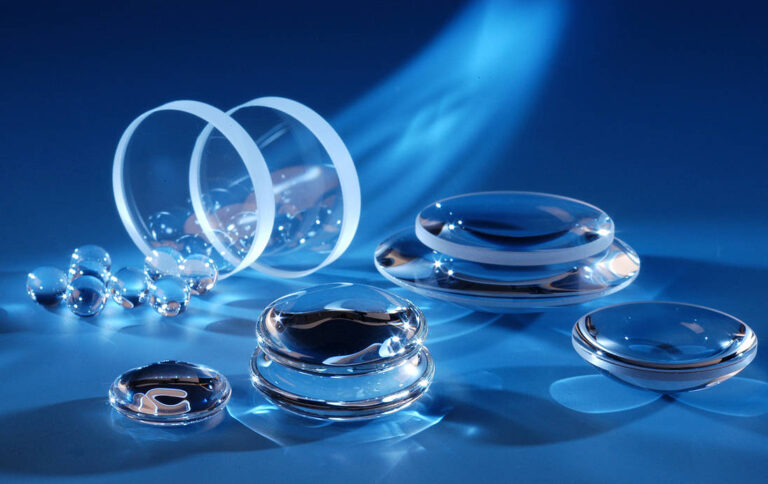
- Optical specifications often require Ra ≤ 1nm: YISHUN Optical achieves Ra 1nm surface roughness through advanced polishing processes
- Measurement technique matters: Different profilometers and interferometers may report Ra or RMS, requiring careful interpretation
- Both metrics are valid but serve different purposes: Ra is industry-standard for general machining; RMS is preferred for optical and vibrational analysis applications
What is Ra (Arithmetical Mean Roughness)?
Ra represents the arithmetic average of the absolute values of the surface height deviations measured from a centerline over a specified evaluation length. Mathematically, it is expressed as:
Ra = (1/n) × Σ|yᵢ|
Where yᵢ represents the vertical deviation from the centerline at each measurement point.
Ra provides a single number that describes the overall roughness amplitude. It is relatively insensitive to occasional large peaks or valleys because it treats all deviations equally regardless of their direction. This makes Ra excellent for describing general surface texture quality and is why it has become the dominant specification in manufacturing environments.
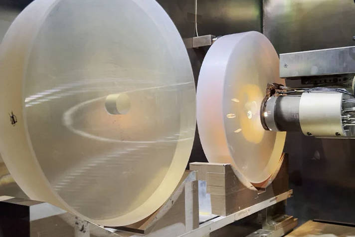
In precision optics, Ra specifications typically appear in aerospace, semiconductor, and medical device applications where surface consistency matters more than peak characterization. YISHUN Optical’s standard polishing services routinely achieve Ra values below 1nm on glass, silicon, and metal substrates.
Advantages of Ra Measurement
- Simpler calculation and easier to understand
- Less sensitive to occasional surface defects
- Widely adopted standard across manufacturing industries
- Consistent results between different measurement equipment
- Sufficient for most general precision requirements
What is RMS (Root Mean Square Roughness)?
RMS roughness calculates the root mean square of the vertical deviations from the centerline. The formula is:
RMS = √[(1/n) × Σyᵢ²]
This mathematical approach squares each deviation before averaging, which amplifies the significance of larger deviations. A surface with sharp peaks or deep scratches will show a much higher RMS value compared to Ra, making RMS more sensitive to surface anomalies.
For optical applications, RMS is often preferred because scattered light intensity correlates more closely with RMS roughness than Ra. Optical scatter is proportional to the square of surface irregularity amplitude, so surfaces with occasional high peaks—barely affecting Ra—can cause disproportionate light scatter detected by RMS measurement.
When RMS Matters More Than Ra
- Laser gyroscope mirrors: Scattered light causes bias drift
- Interferometer reference surfaces: Path length errors from surface irregularities
- Semiconductor lithography optics: Scatter reduces image contrast
- High-power laser optics: Localized intensity spikes from surface peaks
The Mathematical Relationship: Ra vs RMS
For surfaces following a Gaussian distribution—a common assumption for machined and polished surfaces—the theoretical relationship between Ra and RMS is:
RMS ≈ 1.11 × Ra
This means RMS values are approximately 11% higher than Ra values for the same surface under ideal conditions. However, real-world surfaces rarely exhibit perfect Gaussian distributions. Surfaces with occasional scratches, tool marks, or processing artifacts will show larger disparities between Ra and RMS measurements.
| Surface Type | Typical Ra | Expected RMS | Ratio |
|---|---|---|---|
| Diamond-turned metal | 5-20 nm | 6-25 nm | 1.10-1.25 |
| Ground glass | 50-200 nm | 60-250 nm | 1.10-1.30 |
| Polished glass | 0.5-2 nm | 0.6-2.5 nm | 1.10-1.25 |
| Super-polished optics | 0.1-0.5 nm | 0.12-0.65 nm | 1.15-1.35 |
Measurement Techniques for Optical Components
Contact Profilometry
Stylus-based profilometers physically trace the surface with a diamond tip (typically 2μm radius). These instruments provide highly repeatable Ra and RMS measurements and can profile across steps, edges, and features. Limitations include potential surface damage from the stylus and inability to measure extremely soft materials.
Interferometric Microscopy
White-light interferometers and phase-shifting interferometers measure surface height optically without contact. These systems achieve sub-nanometer resolution and are ideal for sensitive optical surfaces. Multiple passes and stitching techniques extend measurement range while maintaining precision.
Atomic Force Microscopy (AFM)
For sub-nanometer roughness measurements, AFM provides true 3D surface mapping at atomic resolution. However, scan areas are limited (typically < 100μm × 100μm), making AFM suitable for research rather than production characterization.
Why Surface Roughness Matters in Optics
Light Scatter and Transmission Loss
Every surface irregularity that exceeds the wavelength of light scatters radiation out of the intended beam path. For visible light (400-700nm wavelength), surface features larger than λ/10 (40-70nm) become significant scatter sources. A surface with Ra 10nm scatters approximately 100 times more light than a surface with Ra 1nm.
Laser-Induced Damage Threshold (LIDT)
High-peak-power laser systems are particularly sensitive to surface roughness. Electric field intensification at surface peaks can initiate laser-induced damage at fluences far below the bulk material’s damage threshold. Ultra-polished surfaces with minimal micro-roughness enable higher LIDT ratings.
Wavefront Distortion
In imaging systems, surface roughness contributes to wavefront error that degrades resolution and contrast. For astronomical telescopes and lithography tools, accumulated surface errors across multiple optical elements determine ultimate system performance.
YISHUN Optical’s Surface Roughness Capabilities

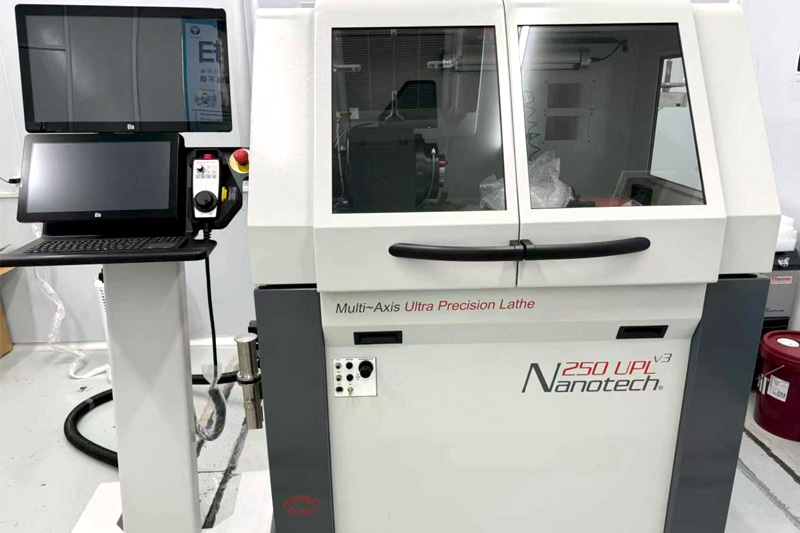
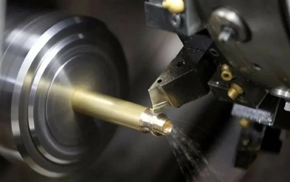
With over 20 years of experience in precision optical manufacturing, YISHUN Optical has developed advanced polishing processes capable of achieving Ra ≤ 1nm surface roughness consistently across production volumes. Our capabilities include:
- Computer-Controlled Polishing (CCP): Iterative sub-aperture tool motion with in-process interferometric metrology
- Magneto-Rheological Finishing (MRF): Deterministic material removal for correcting mid-spatial-frequency errors
- Ion Beam Figuring (IBF): Material removal without mechanical contact for ultimate surface quality
- Pitch Polishing: Classical figuring technique for achieving lowest micro-roughness on transmissive optics
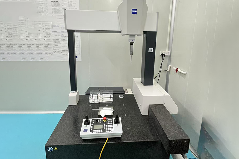
All surface measurements are verified using Zygo interferometers and TalySurf profilometers, with complete traceability to ISO 9001:2015 quality standards. Our metrology laboratory maintains environmental controls to ensure measurement reliability.
Common Specifications and Conversion Guidance
When specifying surface roughness requirements for RFQ or purchase orders, YISHUN Optical recommends:
- Clarify which parameter (Ra or RMS) is required and under what measurement conditions
- Specify evaluation length or area to ensure consistent sampling
- Define measurement technique if results must match another supplier’s data
- Request surface maps or profiles for critical applications beyond single-value specifications
- Include filtering parameters (cutoff wavelengths) if spatial frequency content matters
Frequently Asked Questions
Is Ra or RMS better for specifying optical surfaces?
For most optical applications, Ra is sufficient and is the industry standard for manufacturing specifications. However, when optical performance (especially scatter) is the primary concern, RMS may provide a more meaningful correlation with measured performance. Always specify both values when possible and ensure measurement conditions are documented.
Why do different suppliers report different roughness values for similar parts?
Differences arise from measurement technique (contact vs. optical), evaluation length, filter settings, and the specific area sampled. A single 50μm × 50μm area may not represent an entire 100mm diameter optic. Request measurement location documentation and consider requesting surface maps for critical applications.
Can Ra predict laser damage threshold?
Ra alone is insufficient for LIDT prediction because peak intensity at individual surface features (rather than average roughness) determines damage initiation. However, ultra-low Ra values (< 1nm) generally correlate with good LIDT performance when combined with absence of scratches, digs, and contamination.
What surface roughness is needed for visible light optics?
For general visible light applications (imaging lenses, illumination optics), Ra 3-5nm is typically acceptable. For laser applications or high-resolution imaging, Ra < 1nm may be required. Infrared optics often have relaxed requirements due to longer wavelengths.
How do you verify sub-nanometer roughness claims?
Sub-nanometer roughness should be verified using interferometric microscopy or AFM with documented measurement conditions. Ask for surface PSD (Power Spectral Density) analysis to ensure roughness is distributed across appropriate spatial frequencies, not just low overall Ra values achieved by filtering.
Conclusion
Understanding the distinction between Ra and RMS surface roughness enables more precise specification and evaluation of optical components. While Ra provides a robust, industry-standard metric for general surface quality, RMS offers greater sensitivity to the peak features that dominate optical scatter and laser damage mechanisms.
For demanding applications requiring surface roughness below 1nm, YISHUN Optical’s 20+ years of expertise in precision polishing and advanced finishing techniques—supported by ISO 9001:2015 certified processes and precision metrology equipment—ensures your optical components meet the most stringent performance requirements.
Ready to discuss your optical surface roughness requirements? Contact our engineering team at info@yishunoptical.com or visit yishunoptical.com to request a quote for your next precision optical project.