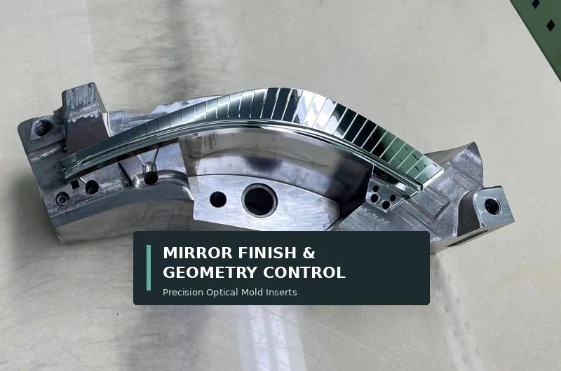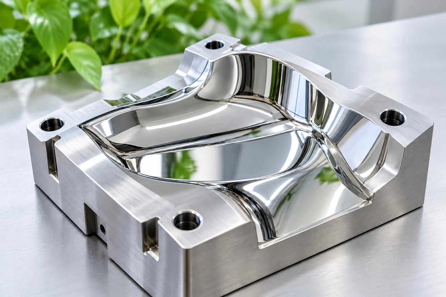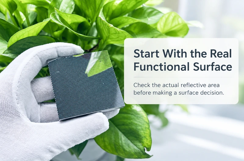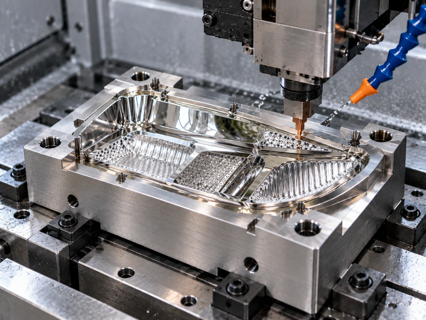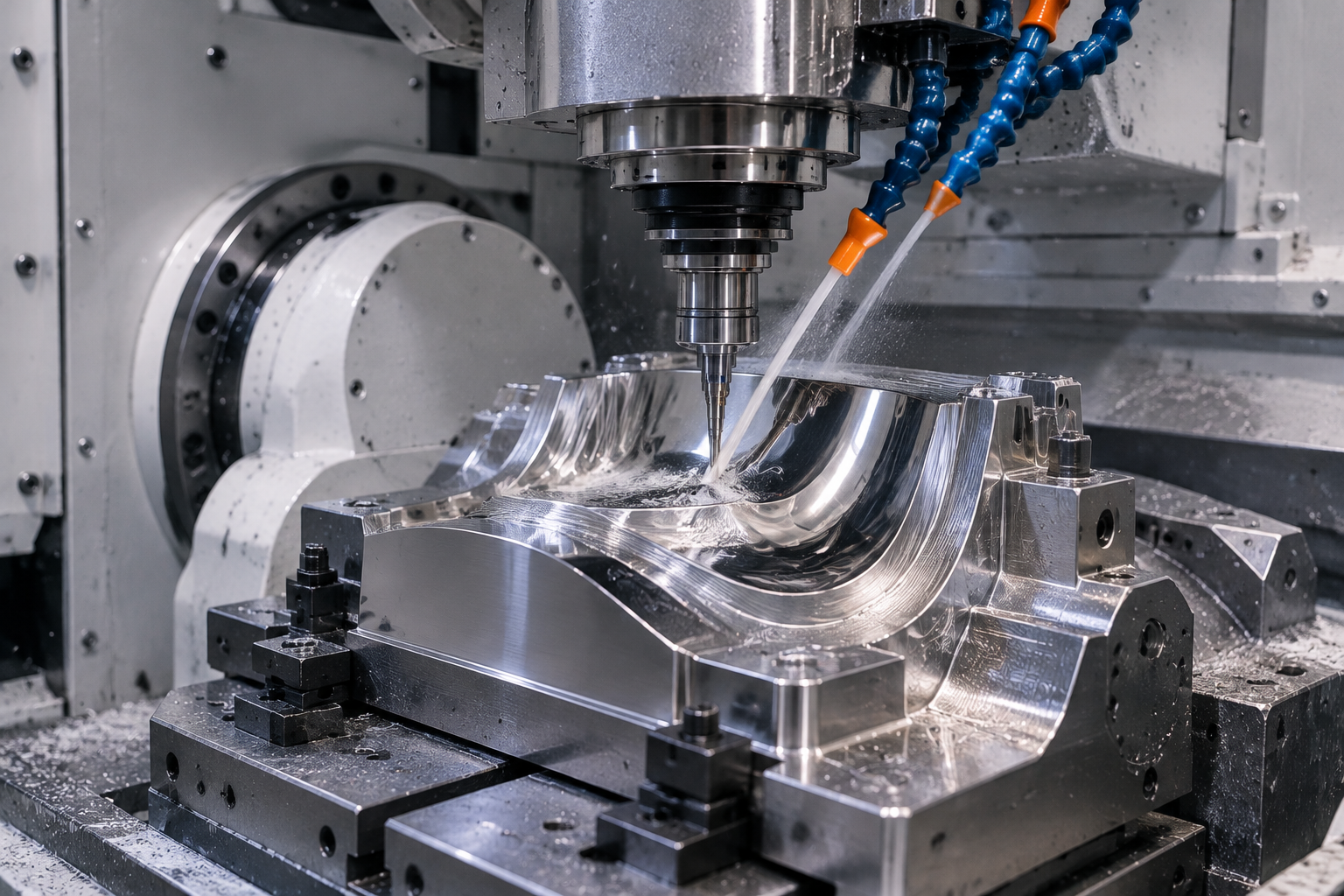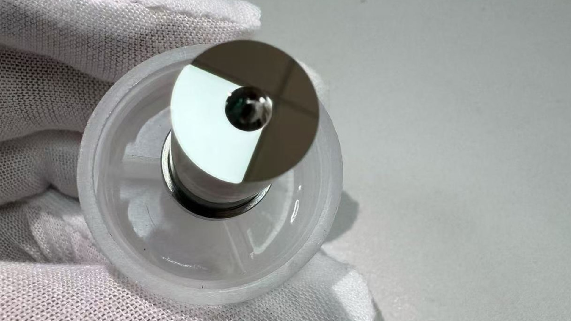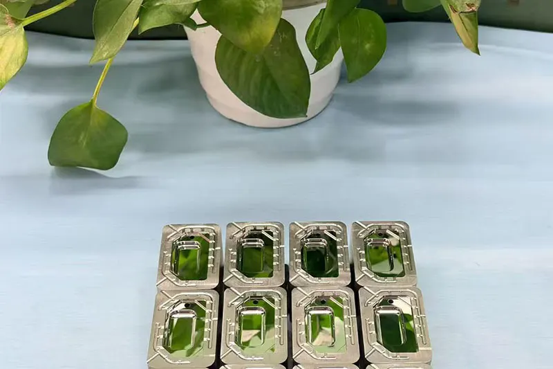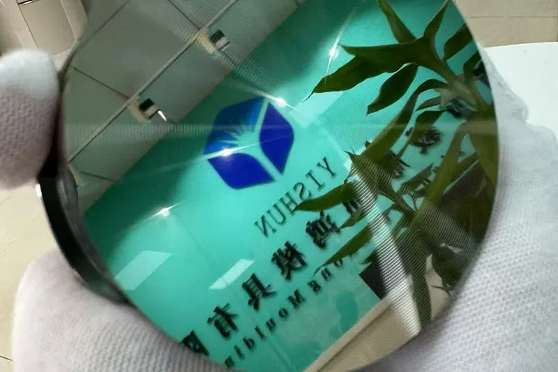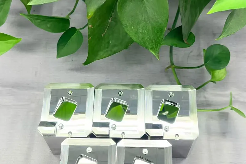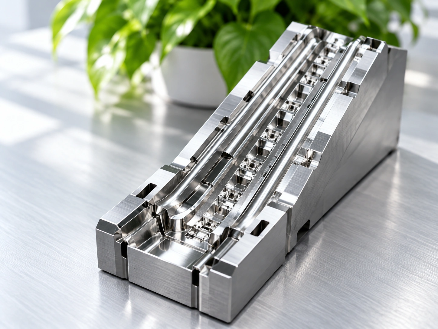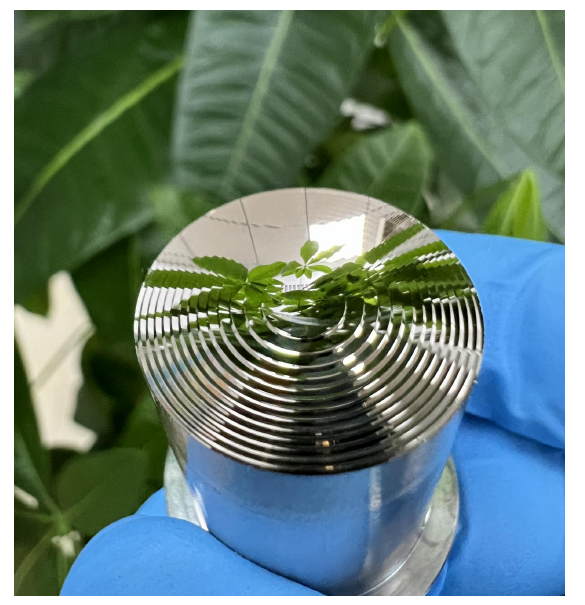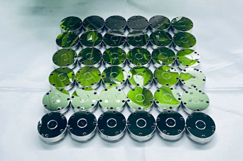
Precision optical polishing is a controlled finishing process used to improve the surface quality, flatness, roughness, and optical performance of components such as lenses, windows, mirrors, prisms, wafers, and precision substrates. It removes fine surface defects left by cutting, grinding, or lapping and helps achieve the optical clarity or reflective performance required in high-precision applications.
For many optical and photonics projects, polishing is not simply a cosmetic finishing step. It directly affects transmission, reflection, scattering, image quality, laser damage resistance, sealing performance, and assembly accuracy. When combined with lapping, precision polishing can help control both the geometry and the final surface finish of optical components.
If your project requires custom optical surfaces, tight flatness, low surface roughness, or controlled scratch-dig quality, working with an experienced optical polishing and lapping services provider can help reduce technical risk during prototyping and production.
What Is Precision Optical Polishing?
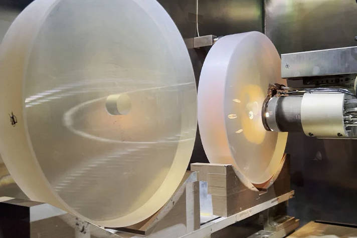
Precision optical polishing is a fine material-removal process used to create smooth, accurate, and defect-controlled optical surfaces. Unlike general polishing, which may only improve appearance, optical polishing focuses on measurable performance parameters such as flatness, parallelism, surface roughness, dimensional tolerance, and surface quality.
The goal of precision optical polishing is to produce a surface that meets defined optical and mechanical specifications, not just a visually smooth finish.
Typical components that may require optical polishing include:
| Component Type | Common Purpose of Polishing |
|---|---|
| Optical windows | Improve transmission and reduce scattering |
| Lenses | Improve imaging performance and surface quality |
| Mirrors | Improve reflectivity and wavefront accuracy |
| Prisms | Maintain optical clarity and angle accuracy |
| Glass substrates | Improve flatness and surface finish |
| Sapphire parts | Improve wear resistance and optical performance |
| Quartz and fused silica components | Support UV, laser, and high-temperature applications |
| Ceramic or silicon components | Improve flatness, sealing, or functional surface quality |
In many projects, optical polishing is performed after cutting, shaping, grinding, or lapping. Lapping helps achieve better flatness, thickness control, and parallelism, while polishing improves the final surface condition.
Why Precision Optical Polishing Matters
For B2B optical components, small surface errors can create large performance problems. A component may have the correct size and shape, but still fail if its surface finish, flatness, or scratch-dig quality does not meet application requirements.
Precision polishing is especially important when components are used in:
- Laser systems
- Imaging devices
- Optical instruments
- Semiconductor equipment
- Photonics modules
- Medical optical devices
- Metrology systems
- High-Reliability Optical Systems optics
- High-precision research equipment
For example, excessive surface roughness may increase light scattering. Poor flatness may affect bonding, sealing, or optical alignment. Surface scratches may reduce transmission or create local stress points. Edge chips may cause assembly issues or reduce long-term reliability.
In optical manufacturing, surface quality is often as important as dimensional accuracy because light interacts directly with the finished surface.
This is why engineering teams usually specify polishing requirements clearly in drawings, RFQs, or technical documents.
Precision Optical Polishing vs. Optical Lapping
Optical polishing and optical lapping are closely related, but they are not the same process. In many precision projects, both are used together.
| Item | Optical Lapping | Optical Polishing |
|---|---|---|
| Main Purpose | Improve flatness, parallelism, and thickness control | Improve surface smoothness, clarity, and optical quality |
| Material Removal | Usually higher than polishing | Very fine material removal |
| Surface Finish | Better than grinding, but may still be matte or semi-finished | Smooth, transparent, reflective, or optical-grade finish |
| Typical Focus | Geometry control | Surface quality control |
| Common Applications | Substrates, wafers, sealing surfaces, flat components | Windows, lenses, mirrors, prisms, optical surfaces |
| Inspection Focus | Flatness, thickness, parallelism | Roughness, scratch-dig, surface defects, optical clarity |
Lapping is commonly used to control geometry, while polishing is used to refine the final optical surface. For parts requiring both accurate geometry and high surface quality, a combined polishing and lapping process is often the most practical approach.
For custom components that require both processes, Yishun Optical provides precision optical polishing and lapping services for a range of optical materials and component geometries.
How the Precision Optical Polishing Process Works
The exact process depends on the material, part geometry, tolerance requirements, and final application. However, a typical precision optical polishing workflow includes the following steps.
1. Drawing and Requirement Review
Before production begins, the supplier reviews the customer’s drawing, material, surface requirements, dimensions, quantities, and inspection criteria. This step is critical because polishing requirements must be realistic, measurable, and aligned with the application.
Important details include:
- Material type
- Part size and thickness
- Required flatness
- Parallelism requirement
- Surface roughness target
- Scratch-dig specification
- Edge quality requirement
- Coating or bonding requirements
- Quantity and delivery schedule
A clear RFQ helps the supplier select the right process and avoid unnecessary cost.
2. Pre-Machining or Grinding
Raw materials are usually cut, shaped, machined, or ground before polishing. This stage prepares the part close to its final dimensions. However, grinding can leave subsurface damage and tool marks, which must be removed by later steps.
3. Lapping for Flatness and Thickness Control
For flat components, lapping may be used to improve flatness, thickness uniformity, and parallelism. This process uses abrasive particles between the workpiece and a lapping plate to remove material in a controlled way.
Lapping is especially useful for optical windows, wafers, glass substrates, quartz plates, sapphire components, and ceramic parts.
4. Fine Polishing
Polishing uses fine abrasives, polishing pads, slurry, and controlled motion to remove micro-level surface defects. The purpose is to achieve the final surface finish and optical clarity.
Key process variables include:
- Polishing pressure
- Pad material
- Abrasive type and particle size
- Slurry chemistry
- Polishing time
- Machine stability
- Operator control
- Cleaning procedure
For high-value optical parts, the polishing process may require several stages, moving from rough polishing to fine polishing.
5. Cleaning and Surface Inspection
After polishing, components must be carefully cleaned to remove slurry, particles, and residues. Inspection then verifies whether the part meets the required specification.
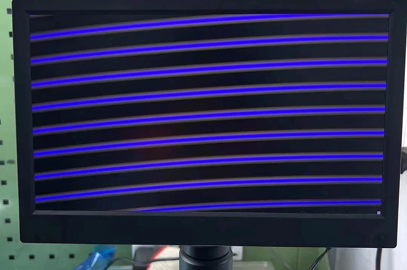
Common inspection methods may include visual inspection, interferometry, profilometry, microscopy, thickness measurement, and surface quality evaluation.
6. Packaging and Handling
Polished optical surfaces are sensitive to scratches, fingerprints, particles, and impact damage. Proper packaging is important to protect the finished components during storage and shipment.
Key Tolerances in Precision Optical Polishing
Precision optical polishing is usually evaluated by several measurable parameters. The exact tolerance depends on the material, part size, geometry, and application.
| Parameter | What It Means | Why It Matters |
|---|---|---|
| Surface Roughness | Microscopic texture of the polished surface | Affects scattering, transmission, reflection, and sealing |
| Flatness | Deviation from a perfectly flat plane | Affects optical alignment, bonding, and contact performance |
| Parallelism | Relationship between two opposite surfaces | Important for windows, plates, substrates, and assemblies |
| Scratch-Dig | Visual surface defect standard for optical parts | Helps control visible scratches and pits |
| Thickness Tolerance | Allowed variation in part thickness | Important for mechanical fit and optical path length |
| Edge Quality | Condition of edges after processing | Reduces chipping risk and handling damage |
| Dimensional Tolerance | Size accuracy of the finished component | Ensures assembly compatibility |
The most important optical polishing tolerances are usually surface roughness, flatness, parallelism, scratch-dig quality, and dimensional accuracy.
In many applications, engineers should avoid specifying unnecessarily tight tolerances. Overly strict requirements can increase cost, lead time, and manufacturing difficulty without improving actual product performance. A qualified supplier can help review the drawing and recommend a practical specification.
Common Materials for Optical Polishing and Lapping
Different materials behave differently during polishing. Hardness, brittleness, thermal expansion, chemical resistance, and internal stress can all affect process selection.
| Material | Typical Polishing Considerations |
|---|---|
| Optical glass | Requires careful control of scratches, chips, and surface roughness |
| Fused silica | Often used in UV, laser, and thermal applications; requires clean processing |
| Quartz | Needs stable polishing for optical clarity and dimensional accuracy |
| Sapphire | Very hard and wear-resistant, but more difficult to lap and polish |
| Silicon | Often requires flatness and surface control for semiconductor-related uses |
| Ceramics | Brittle materials require edge protection and controlled removal |
| Optical crystals | May require special handling depending on orientation and sensitivity |
| Metals for mirrors | May require diamond machining, polishing, or coating preparation |
For a project involving multiple materials, it is important to confirm whether the same supplier can handle both the material and the required surface specification. You can learn more about available service capabilities through Yishun Optical’s custom optical polishing service page.
Applications of Precision Optical Polishing
Precision optical polishing is used wherever surface quality affects optical, mechanical, or functional performance.
Optical Windows
Optical windows protect sensors, lasers, cameras, and instruments while allowing light to pass through. Polishing helps improve transmission and reduce scattering. Flatness and parallelism may also be important when windows are used in precision optical paths.
Lenses and Prisms
For lenses and prisms, polished surfaces influence image clarity, light transmission, and wavefront quality. Poor surface quality can reduce optical performance, especially in imaging and laser systems.
Mirrors and Reflective Components
Mirror substrates require controlled surface quality before coating or final use. Polishing can improve surface finish and prepare the part for reflective coatings.
Semiconductor and Photonics Components
Semiconductor, photonics, and sensor industries often require precise flatness and smooth surfaces for wafers, substrates, carriers, and optical interfaces.
Laser Systems
Laser optics can be sensitive to surface defects, contamination, and roughness. Proper polishing and cleaning help reduce scattering and support stable optical performance.
Metrology and Scientific Instruments
Precision measurement systems often rely on stable optical surfaces. Polishing quality can affect repeatability, alignment, and measurement accuracy.
Factors That Affect Polishing Quality
Several variables influence the final result of precision optical polishing.
Material Properties
Hard, brittle, or chemically sensitive materials may require slower processing and tighter control. Sapphire, ceramics, and fused silica often require different polishing strategies than standard optical glass.
Starting Surface Condition
The quality of the ground or lapped surface affects polishing time and final quality. If subsurface damage is too deep, polishing alone may not remove it efficiently.
Part Geometry
Thin, large, or irregularly shaped parts are more difficult to polish without deformation. Fixtures and process planning become more important for these components.
Flatness and Thickness Requirements
Tight flatness and thickness tolerances require careful lapping, polishing, and inspection. For double-sided components, parallelism control may also be critical.
Cleanliness
Particles, dried slurry, or poor cleaning can create scratches and contamination. Clean handling is especially important for optical, laser, and semiconductor applications.
Inspection Capability
A supplier must be able to measure what it claims to produce. Inspection equipment and process documentation are important parts of supplier evaluation.
Common Mistakes When Specifying Optical Polishing
Many project delays begin with unclear or unrealistic specifications. Below are common mistakes buyers should avoid.
| Mistake | Possible Problem | Better Approach |
|---|---|---|
| Only saying “optical quality” | Too vague for production and inspection | Specify roughness, scratch-dig, flatness, and dimensions |
| Over-tightening all tolerances | Higher cost and longer lead time | Match tolerances to actual application needs |
| Ignoring material behavior | Chipping, warping, or low yield | Discuss material-specific risks with the supplier |
| Not defining inspection method | Disagreement during acceptance | Confirm measurement standards before production |
| Providing incomplete drawings | Rework and quotation delays | Include material, size, quantity, tolerances, and surface requirements |
| Ignoring edge requirements | Chips during handling or assembly | Specify chamfer, bevel, or edge quality if needed |
A successful optical polishing project starts with clear specifications, realistic tolerances, and a supplier that understands both the material and the application.
How to Choose an Optical Polishing Services Supplier
Choosing the right supplier is important because optical polishing is highly process-dependent. A low-cost supplier without suitable inspection capability may create hidden risks, especially for tight-tolerance or high-value components.
When evaluating a supplier, consider the following factors:
Technical Capability
Check whether the supplier has experience with your material, part size, geometry, and required surface quality. A supplier that handles optical glass may not automatically be suitable for sapphire, fused silica, ceramics, or semiconductor-related materials.
Process Range
For many parts, polishing alone is not enough. The supplier may also need lapping, grinding, machining, cleaning, inspection, and packaging capabilities.
Inspection and Quality Control
Ask what inspection methods are available. For precision optical components, visual inspection alone may not be sufficient. Depending on your requirements, the supplier may need flatness measurement, surface roughness measurement, thickness measurement, microscopy, or other inspection methods.
Engineering Communication
A qualified supplier should be able to review your drawing, identify unclear requirements, and suggest practical process options. This is especially valuable during prototype development.
Production Flexibility
Some projects require one-off prototypes, while others need repeatable batch production. Confirm whether the supplier can support your volume and lead time expectations.
For companies looking for custom optical finishing support, Yishun Optical offers optical processing services for precision components used in industrial, optical, and technical applications.
What Information Should You Provide for an RFQ?
To receive an accurate quotation for precision optical polishing, prepare the following information:
| RFQ Information | Why It Is Needed |
|---|---|
| Material | Determines process, abrasives, and polishing difficulty |
| Drawing or CAD file | Defines dimensions, tolerances, and geometry |
| Quantity | Affects process planning and pricing |
| Surface roughness | Defines final surface finish requirement |
| Flatness | Determines lapping and polishing control |
| Parallelism | Important for plates, windows, and substrates |
| Scratch-dig requirement | Defines visual surface quality |
| Edge specification | Helps prevent chipping and handling issues |
| Application | Helps supplier understand functional priorities |
| Inspection requirement | Defines acceptance criteria |
If you are not sure what tolerance to specify, it is better to describe the application and performance requirement first. The supplier can then help recommend a practical polishing and inspection approach.
Conclusion
Precision optical polishing is a critical finishing process for components that require controlled surface quality, flatness, roughness, and optical performance. It is widely used for optical windows, lenses, mirrors, prisms, wafers, substrates, laser components, semiconductor parts, and precision instruments.
For engineering and procurement teams, the key is to define requirements clearly. Material, surface roughness, flatness, parallelism, scratch-dig, edge quality, and inspection methods all affect cost, lead time, and final performance.
If your project requires custom optical surfaces, tight geometry control, or reliable finishing for technical components, Yishun Optical can support your project with optical polishing and lapping services from requirement review to finished part delivery.
FAQ
What is precision optical polishing used for?
Precision optical polishing is used to improve the surface quality, roughness, flatness, and optical performance of components such as lenses, windows, mirrors, prisms, substrates, and wafers. It is common in laser systems, photonics, semiconductor equipment, imaging devices, and precision instruments.
What is the difference between optical polishing and lapping?
Optical lapping mainly controls flatness, thickness, and parallelism, while optical polishing improves the final surface finish and optical quality. Many precision components require both lapping and polishing to meet geometry and surface requirements.
What tolerances are important in optical polishing services?
Important tolerances include surface roughness, flatness, parallelism, scratch-dig quality, thickness tolerance, dimensional accuracy, and edge quality. The most suitable tolerance depends on the material, component design, and application.
What materials can be used for precision optical polishing?
Common materials include optical glass, fused silica, quartz, sapphire, silicon, ceramics, optical crystals, and some metal mirror substrates. Each material requires a suitable polishing process based on hardness, brittleness, and surface requirements.
How do I request a quote for optical polishing and lapping services?
To request a quote, provide the material, drawing, dimensions, quantity, surface roughness, flatness, parallelism, scratch-dig requirement, edge specification, and intended application. Clear specifications help the supplier provide a more accurate process plan and quotation.
Why is surface roughness important in precision optical polishing?
Surface roughness affects light scattering, transmission, reflection, sealing performance, and coating quality. Lower roughness is often required for optical, laser, and high-precision measurement applications.
Can polishing fix all scratches or defects on an optical component?
Polishing can remove many fine surface defects, but deep scratches, chips, cracks, or subsurface damage may require additional grinding or may not be repairable. The supplier should inspect the part before confirming whether rework is possible.