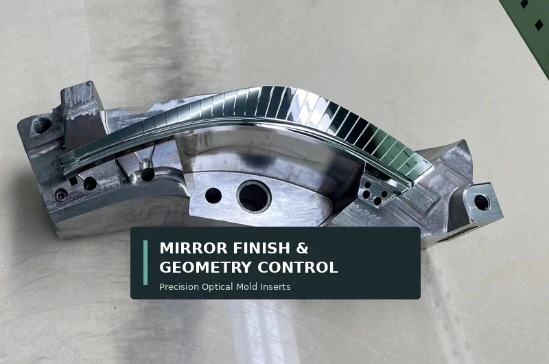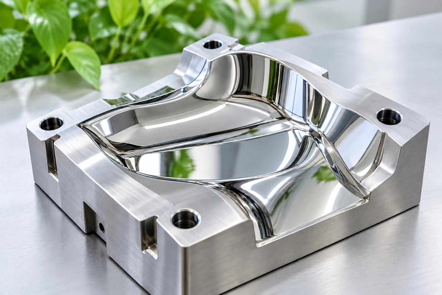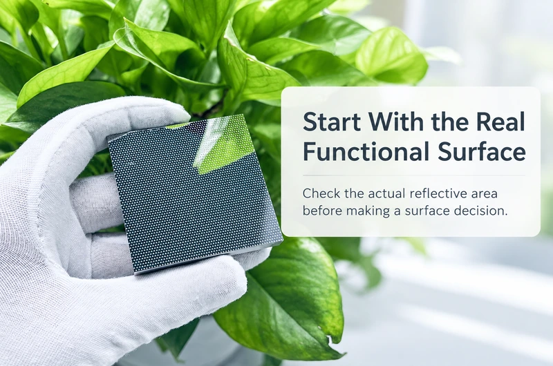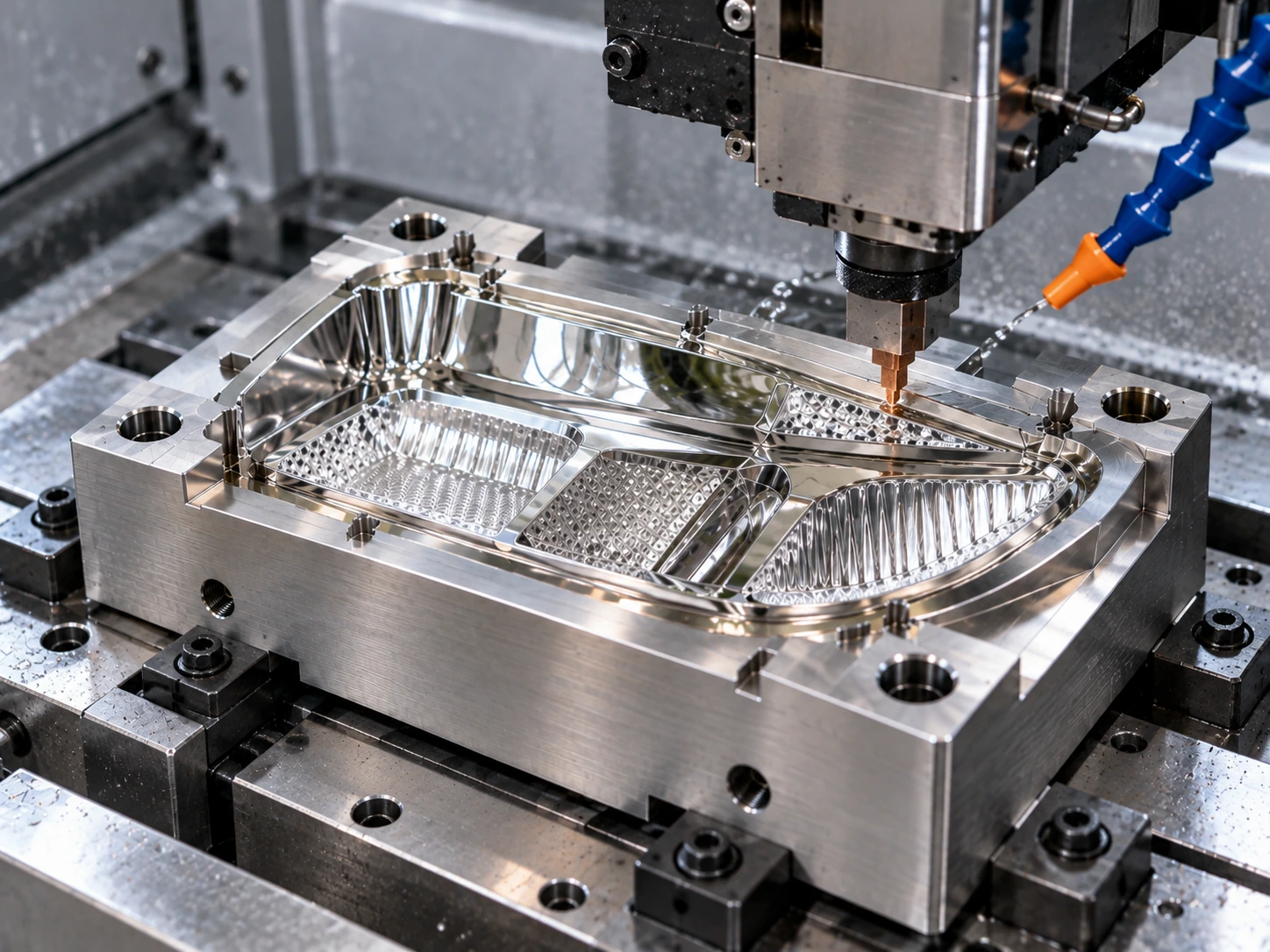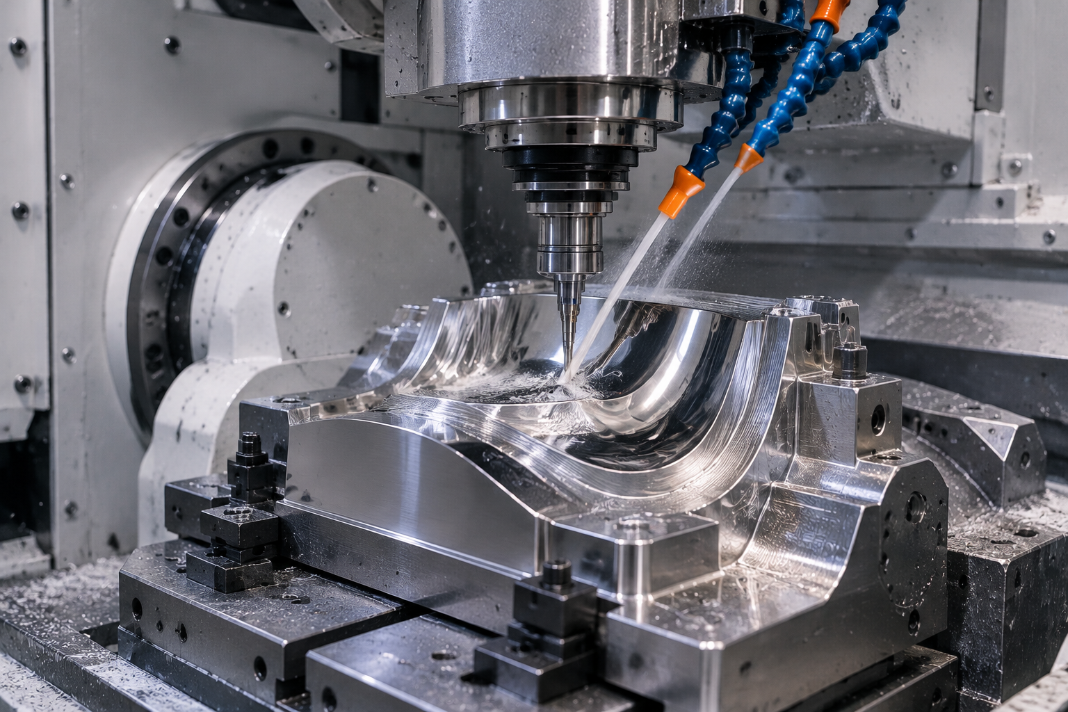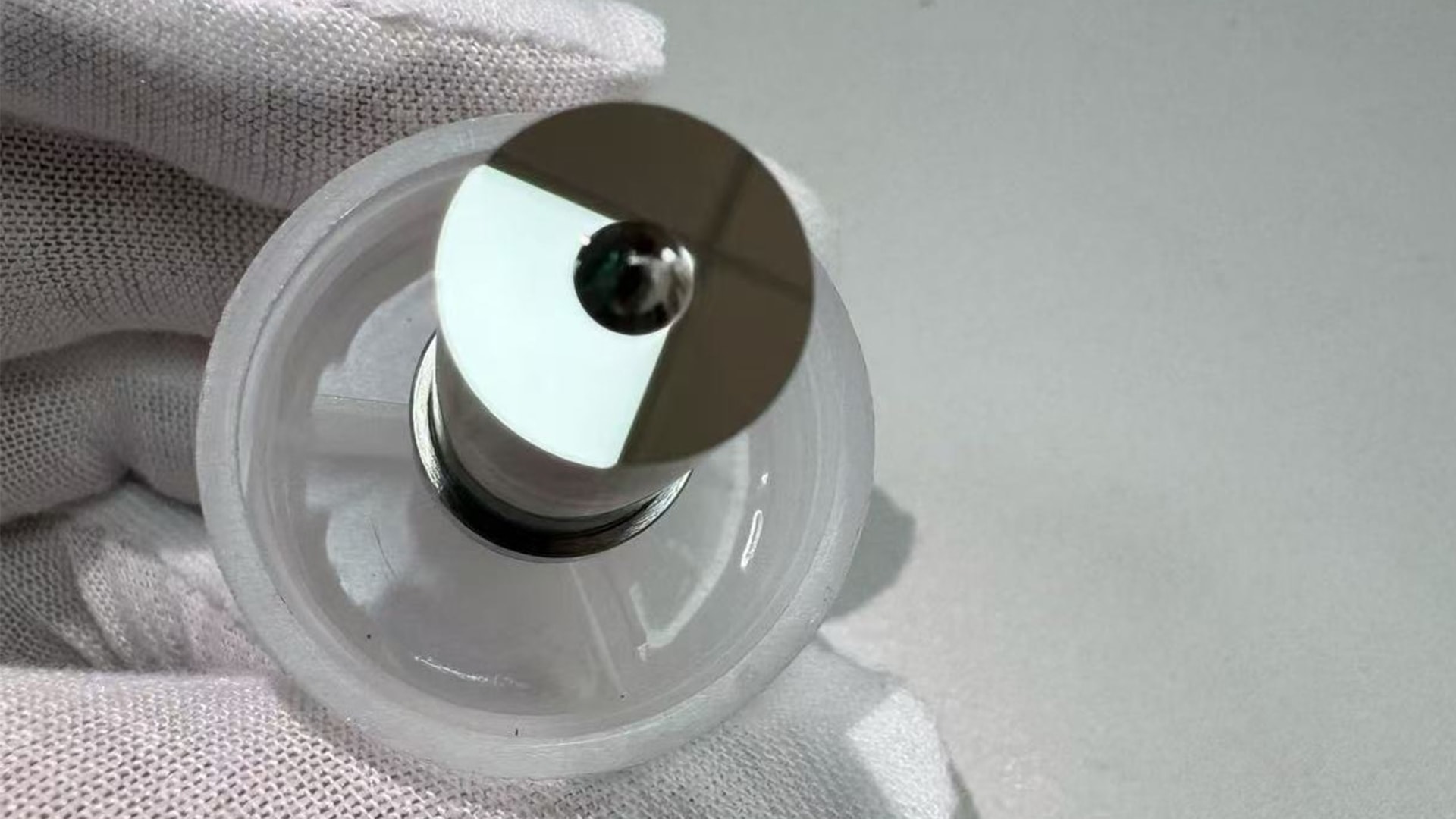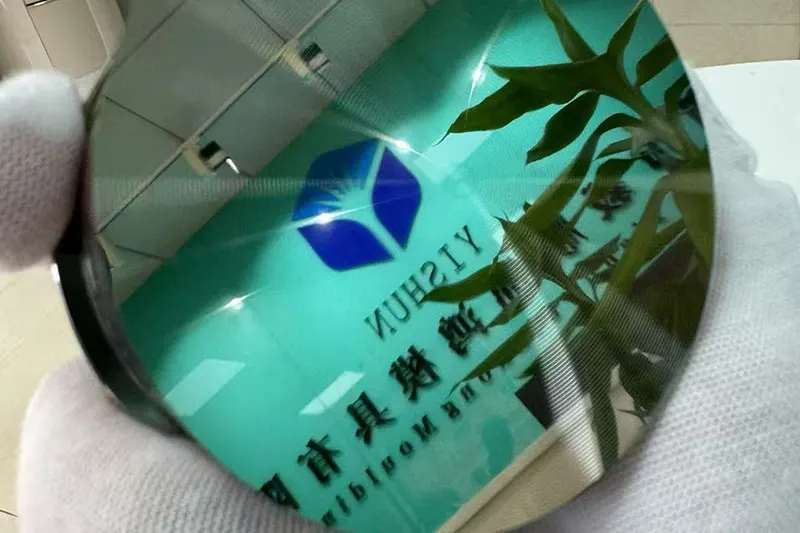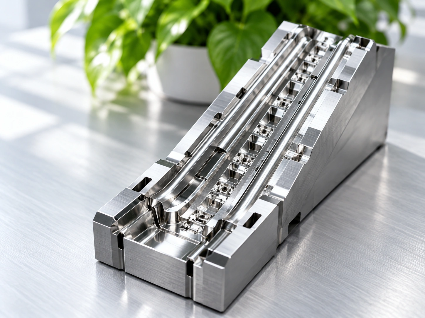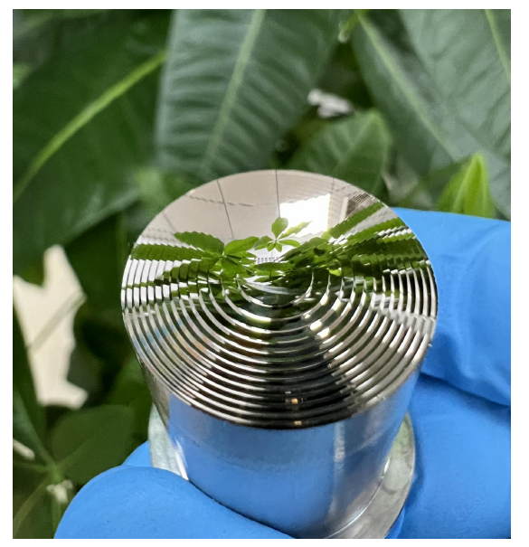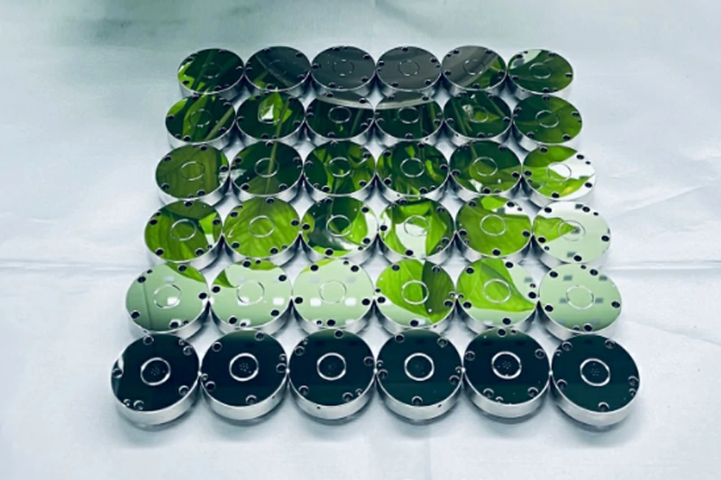

Single Point Diamond Turning (SPDT) represents one of the most precise manufacturing processes available for creating optical-quality surfaces on metal, plastic, and semiconductor materials. This ultra-precision machining technique uses a naturally occurring or synthetic diamond as the cutting tool, operating in a controlled environment to produce surfaces with nanometer-level form accuracy and sub-nanometer surface roughness. The technology enables manufacturers to produce complex optical components without requiring expensive mold tooling or multi-stage polishing operations.
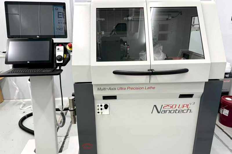
For engineers and procurement specialists evaluating SPDT as a manufacturing solution, understanding the process capabilities, limitations, and optimal applications is essential for making informed sourcing decisions. YISHUN Optical’s SPDT capabilities, powered by Moore Nanotech 250 UPL diamond turning machines and 20+ years of expertise, demonstrate how this technology serves demanding optical applications across high-reliability optical, medical, and consumer electronics sectors.
Key Takeaways
- SPDT achieves both form accuracy (λ/10) and surface roughness (Ra < 1nm) in a single operation, eliminating multiple grinding and polishing steps
- Diamond tool life typically spans 100-500 hours of cutting time depending on material and conditions
- Compatible materials include aluminum alloys, copper, germanium, zinc sulfide, silicon, and various optical plastics
- Environmental controls (temperature stability, vibration isolation, humidity) are critical for achieving full machine precision
- Post-processing options may still be required for highest-performance applications or transmissive optics
What is Single Point Diamond Turning?
Single Point Diamond Turning is a precision machining process where a single-crystal or polycrystalline diamond tool with a precisely controlled geometry removes material from a rotating workpiece. The process occurs on specialized ultra-precision CNC machines (often called diamond turning centers) that provide:
- Sub-micrometer positioning accuracy through aerostatic spindles and linear motors
- Nanometer-level servo control with closed-loop feedback systems
- Thermal stability maintained within ±0.1°C in climate-controlled enclosures
- Vibration isolation from environmental and machinery sources
- In-process interferometric metrology for real-time surface verification
The diamond tool itself is fabricated from natural or synthetic diamond, with edge radii ranging from 0.1μm to 3μm depending on application requirements. Tool geometry—including rake angle, clearance angle, and nose radius—is optimized for specific materials and surface specifications.
SPDT vs. Conventional Machining
Unlike conventional CNC machining, SPDT operates under fundamentally different constraints:
| Parameter | Conventional Machining | SPDT |
|---|---|---|
| Positioning accuracy | 1-50 μm | 0.01-0.1 μm |
| Surface roughness | 0.1-10 μm Ra | < 0.001 μm Ra |
| Spindle runout | 1-10 μm | < 0.05 μm |
| Environment | Standard workshop | Temperature-controlled cleanroom |
| Tool material | Carbide, ceramic, HSS | Single-crystal diamond |
The SPDT Process: Step by Step
1. Machine Setup and Calibration
Before cutting begins, the SPDT machine undergoes extensive calibration procedures:
- Spindle verification: Radial and axial runout measured using capacitive sensors, typically requiring < 50nm total indicated runout
- Axis orthogonalization: Squareness between X, Z, and C axes verified to within 1 arc-second
- Tool setting: Diamond tool positioned using optical microscopes or in-process probes to ±0.5μm positioning accuracy
- Environmental stabilization: Machine warmed to thermal equilibrium over 4-12 hours with continuous temperature monitoring
2. Workpiece Preparation
Workpiece material selection significantly impacts SPDT outcomes:
- Aluminum alloys (6061, 7075, 2024): Most common for reflective optics; achievable Ra 5-20nm depending on alloy
- Electroless nickel: Plated onto tooling to enable diamond-compatible surfaces with Ra 10-30nm
- Copper and brass: Excellent thermal conductivity optics; Ra 15-50nm typical
- Germanium and silicon: Infrared optics materials with Ra 20-50nm capability
- Zinc sulfide (ZnS): Long-wave IR applications; Ra 30-80nm achievable
- Optical plastics (PMMA, PC, COC): Prototype and consumer optics; Ra 30-100nm
3. Cutting Parameters Optimization
Optimal cutting parameters balance surface quality, tool life, and throughput:
- Depth of cut: 1-50μm for finish passes, up to 500μm for roughing
- Feed rate: 1-20μm/rev depending on desired surface texture
- Spindle speed: 500-3000 RPM based on workpiece diameter
- Cutting fluid: Mineral oil or specialized SPDT fluids; some materials cut dry
4. Surface Generation
The diamond tool generates the surface through a combination of:
- Ploughing: Elastic-plastic deformation at tool edge
- Cutting: Chip formation with discrete material removal
- Spring-back: Elastic recovery of workpiece material after tool passage
The resulting surface consists of microscopic tool marks (feed marks) that become the primary surface texture characteristic. Feed rate directly determines feed mark spacing and affects both aesthetic appearance and functional performance.
5. Post-Processing Verification
YISHUN Optical verifies SPDT surfaces using:
- Zygo interferometers: Form accuracy (λ/10 to λ/20 PV typical)
- TalySurf profilometers: Surface roughness (Ra/RMS) measurement
- CMM inspection: Dimensional verification of complex geometries
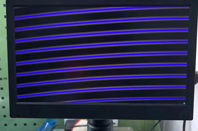
- Surface video microscopy: Defect detection (scratches, digs, tool marks)
Advanced SPDT Configurations

Raster Cutting
The diamond tool traverses in linear passes perpendicular to the spindle rotation, producing concentric tool marks. This technique works well for flat surfaces, spherical lenses, and rotationally symmetric aspheres.
Fast Tool Servo (FTS)
FTS systems add a high-bandwidth linear actuator to the Z-axis, enabling diamond turning of non-rotationally symmetric features including:
- Diffractive optical elements (DOE): Gratings, phase plates, beam splitters
- Micro-optics: Microlens arrays, micro-mirrors
- Freeform surfaces: Off-axis aspheres, generalized Hartmann plates
FTS systems operate at frequencies up to 500Hz with stroke ranges of 0.5-2mm, enabling complex surface features to be diamond turned directly.
Slow Slide Servo (SSS)
SSS configuration uses slow traverse rates (0.1-5mm/min) with continuous Z-axis correction to generate extreme aspheric departures or complex mathematical surfaces. Common applications include ophthalmic lens molds and specialized laser cavity optics.
Surface Characteristics and Performance
Feed Mark Topology
SPDT surfaces exhibit characteristic sinusoidal feed marks with amplitude determined by:
- Feed rate: Higher feeds produce deeper marks
- Tool nose radius: Larger radii produce shallower marks
- Cutting conditions: Vibration, thermal effects, tool wear
For reflective applications, feed marks create anisotropic scattering that can affect polarization performance. The feed mark spatial frequency also determines whether scattered light falls within system acceptance angles.
Subsurface Damage
Unlike brittle materials (glass, ceramics), ductile-regime cutting of metals produces minimal subsurface damage. The plastic deformation zone extends only 10-50nm below the machined surface, enabling excellent fatigue performance and coating adhesion.
Ductile vs. Brittle Material Behavior
The critical depth of cut (Dc) defines the transition between ductile cutting (ploughing) and brittle fracture:
| Material | Critical Depth (nm) | Typical SPDT Quality |
|---|---|---|
| Aluminum | > 500 | Excellent (Ra 5-20nm) |
| Copper | > 300 | Excellent (Ra 15-50nm) |
| Germanium | 50-100 | Good (Ra 20-50nm) |
| Silicon | 30-80 | Moderate (Ra 30-80nm) |
| ZnS | 100-200 | Good (Ra 30-80nm) |
Applications of SPDT Technology
High-Reliability Optical Systems
- Laser gyroscope mirrors: Ultra-low scatter requirements for navigation systems
- Infrared optical systems: Germanium and silicon aspheric lenses for thermal imaging
- high-precision optics: Lightweight aluminum mirrors for high-precision optical instruments applications
- HUD projectors: Precision optical elements for head-up displays
Medical Devices
- Intraocular implants: Aspheric lenses for premium IOLs
- Laser surgical systems: Collimating and focusing optics
- Diagnostic equipment: Flow cytometry optics, microscopy objectives
- Dental imaging: Intraoral scanner optics and illumination
Consumer Electronics
- Smartphone camera components: Compact aspheric lenses for miniaturized optics
- LED lighting: Reflectors and light guides for efficient illumination
- AR/VR headsets: Waveguide combiners and projection optics
- Fingerprint sensors: Protective windows with anti-reflection coatings
Industrial and Scientific
- Semiconductor lithography: Reticle and wafer handling components
- Metrology instruments: Reference surfaces and calibration standards
- Telescope optics: Prototype aspheric mirrors for astronomical research
- Laser machining: Beam delivery optics for materials processing
SPDT Limitations and Considerations
Material Restrictions
- Glass: Cannot be diamond turned (brittle fracture); requires alternative processes
- Ceramics: Limited to specialized compositions with sufficient fracture toughness
- Hard coatings: Diamond-like carbon (DLC) may cause excessive tool wear
- Abrasive materials: Tungsten carbide and similar materials damage diamond tools
Surface Finish Constraints
- Minimum Ra achievable depends on material; some applications require post-SPDT polishing
- Feed marks are inherent to the process; cannot be eliminated without additional processing
- Tool wear effects become visible after extended cutting, requiring tool replacement
Environmental Sensitivity
- Vibration isolation critical for achieving specified form accuracy
- Temperature stability required during cutting and measurement
- Cleanliness essential to prevent contamination affecting surface quality
YISHUN Optical’s SPDT Capabilities
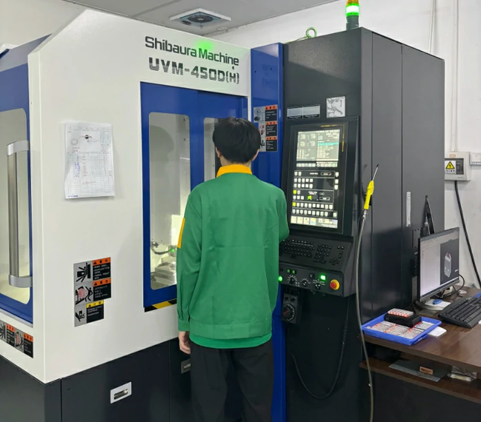
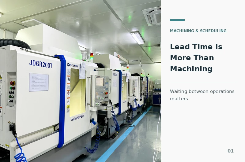
YISHUN Optical operates Moore Nanotech 250 UPL diamond turning centers alongside complementary ultra-precision grinding and polishing equipment. Our SPDT capabilities include:
- Maximum workpiece diameter: 250mm
- Form accuracy: Better than λ/10 (632.8nm) PV typical
- Surface roughness: Ra < 10nm standard, Ra < 1nm achievable on aluminum
- Material range: Aluminum, copper, brass, nickel-phosphorus, germanium, silicon, optical plastics
- Complex features: FTS capability for diffractive and freeform optics
Combined with ISO 9001:2015 and ISO 14001:2015 certification, YISHUN Optical delivers SPDT components meeting the demanding requirements of clients including major high-reliability optical, medical device, and consumer electronics manufacturers.
Frequently Asked Questions
What materials can be diamond turned?
Common SPDT materials include aluminum alloys (6061, 7075), copper, brass, electroless nickel, germanium, silicon, zinc sulfide, and various optical plastics (PMMA, PC, COC). Glass and ceramics generally cannot be diamond turned due to brittle fracture behavior.
Can SPDT produce optical-quality transmissive surfaces?
SPDT produces excellent reflective surfaces directly. Transmissive optics require post-SPDT polishing or must be made from materials suitable for single-point diamond turning. Some infrared materials (germanium, silicon, ZnS) can be diamond turned for transmissive applications.
How long does a diamond tool last?
Diamond tool life varies from 100-500+ hours depending on material, cutting conditions, and surface requirements. Abrasive materials or interrupted cuts significantly reduce tool life. YISHUN monitors tool wear continuously to maintain surface quality throughout production runs.
What is the difference between SPDT and precision grinding?
SPDT uses a diamond cutting edge for material removal, producing excellent surface finishes without subsurface damage. Precision grinding uses abrasive wheels and may induce subsurface damage, but can process harder materials including glass and ceramics.
Does SPDT require post-polishing?
For many applications, SPDT surface quality is sufficient without additional processing. High-performance optics requiring sub-nanometer roughness or lowest-possible scatter may require post-SPDT polishing using MRF or pitch polishing techniques.
What surface accuracy can SPDT achieve?
Modern SPDT machines achieve form accuracy better than λ/10 PV (63nm) routinely, with λ/20-λ/50 achievable under optimal conditions. This accuracy applies to spherical, aspheric, and controlled freeform surfaces.
Conclusion
Single Point Diamond Turning provides an extraordinary combination of form accuracy, surface finish, and production flexibility for precision optical components. The process enables direct generation of aspheric and complex surfaces on suitable materials, reducing lead times and tooling costs compared to conventional grinding-and-polishing approaches.
For applications requiring Ra < 1nm to Ra < 10nm surface finishes with λ/10 form accuracy, SPDT represents an established, production-proven manufacturing technology. YISHUN Optical’s 20+ years of SPDT expertise, Moore diamond turning equipment, and comprehensive quality system ensure your optical components meet demanding specifications.
Explore SPDT capabilities for your optical requirements? Contact YISHUN Optical at info@yishunoptical.com or visit yishunoptical.com to discuss your next project with our engineering team.