Understanding Subsurface Damage in Optical Polishing and How to Avoid It
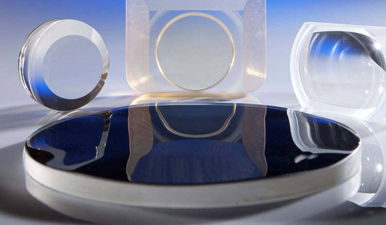
Subsurface damage (SSD) represents one of the most critical yet often overlooked defects in precision optical components. While surface roughness specifications like Ra 1nm capture immediate surface quality, subsurface damage optical polishing processes can introduce hidden structural defects that compromise component performance, longevity, and reliability under operational stress.
For optical engineers and procurement specialists, understanding SSD is essential for specifying appropriate manufacturing processes, selecting qualified suppliers, and ensuring optical systems perform as designed in demanding applications—from semiconductor lithography to aerospace sensors.
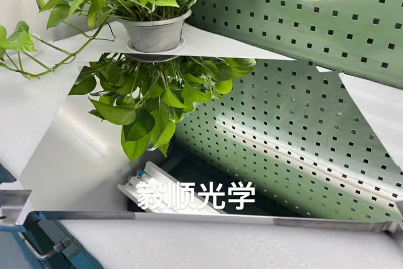
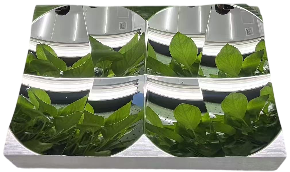
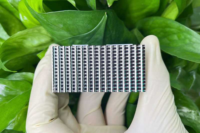
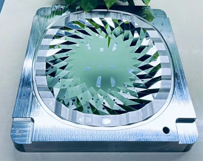
YISHUN Optical’s 20+ years of precision optical manufacturing experience encompasses comprehensive SSD management, combining advanced detection capabilities with optimized process parameters that minimize damage introduction.
Key Takeaway:
- Subsurface damage consists of micro-cracks, dislocation networks, and residual stress extending 0.1-50μm below the polished surface
- SSD degrades laser-induced damage threshold (LIDT), causes birefringence, and reduces mechanical stability
- Both grinding and polishing processes introduce SSD; each requires distinct mitigation strategies
- Detection methods include chemical etching, acoustic microscopy, and cross-sectional TEM analysis
- Process optimization and proper grit progression effectively minimize SSD to acceptable levels
What Is Subsurface Damage in Optical Components?
Subsurface damage refers to structural alterations in optical materials that extend below the visible surface into the subsurface region. These defects manifest as:
Types of Subsurface Defects
- Micro-Cracks: Brittle fracture patterns extending from the surface into the material, ranging from 1-50μm in depth depending on processing conditions
- Dislocation Networks: Crystallographic lattice disturbances created by mechanical stress during material removal
- Compressive/Tensile Residual Stress: Stored elastic energy in the subsurface layer that can cause dimensional instability
- Compacted Layer: Densely packed material zone created by plastic deformation during grinding operations
- White Layer: Amorphous or nanocrystalline surface layer formed through thermomechanical processing
The combined effect of these defects compromises optical performance, particularly in high-power laser applications where SSD serves as initiation points for laser-induced damage.
Why Subsurface Damage Matters: Performance Implications
Understanding why SSD matters requires examining its impact across multiple performance parameters:
Laser-Induced Damage Threshold (LIDT)
In laser optics, SSD directly correlates with reduced LIDT. Micro-cracks and dislocation networks concentrate electromagnetic field energy, creating localized “hot spots” where damage initiates at power levels far below the intrinsic material damage threshold. Research demonstrates that well-polished surfaces without detectable SSD achieve LIDT values 2-5× higher than components with comparable surface roughness but significant subsurface damage.
Birefringence and Polarization Effects
Residual stress in the subsurface layer induces birefringence, causing polarization changes in transmitted light. For precision polarimetric applications, semiconductor inspection systems, and optical metrology, even small birefringence values (λ/50 or less) can introduce measurement errors.
Mechanical Stability
Components with significant SSD exhibit reduced mechanical stability under thermal cycling, vibration, and operational stress. Micro-cracks can propagate under thermal expansion mismatch or mechanical loading, causing catastrophic failure in mission-critical applications.
Scatter Losses
While surface roughness contributes to scatter losses, subsurface defects near the surface also scatter light, degrading system throughput and contrast ratios in imaging systems.
SSD Introduction Sources in Manufacturing
Subsurface damage originates primarily during two manufacturing phases: grinding and polishing. Understanding each source enables targeted mitigation.
Grinding-Induced Subsurface Damage
Grinding operations introduce the most significant SSD layer. Abrasive grit sizes in grinding wheels directly correlate with damage depth:
| Grit Size | Typical Max SSD Depth | Typical RMS Surface |
|---|---|---|
| 60 mesh | 20-50 μm | 800-1200 nm |
| 120 mesh | 8-20 μm | 300-600 nm |
| 240 mesh | 3-8 μm | 100-300 nm |
| 400 mesh | 1-3 μm | 40-100 nm |
| 600 mesh | 0.5-1.5 μm | 20-50 nm |
The grinding process creates subsurface damage through three primary mechanisms:
- Indentation Fracture: Grit particles indent the surface under grinding pressure, creating median and lateral cracks extending into the material
- Abrasion: Sliding contact between grit and surface removes material through micro-cutting and plastic flow
- Thermal Effects: Frictional heating causes localized thermal expansion and resulting thermomechanical damage
Polishing-Induced Subsurface Damage
While polishing removes material at much lower rates than grinding, improper polishing processes can introduce additional SSD:
- Agglomerated Abrasive Particles: Oversized or agglomerated polishing compound particles cause excessive local pressure and micro-crack formation
- Chemical-Mechanical Effects: Inappropriate pH or chemical composition of polishing slurries can accelerate crack propagation
- Pad Hardness Mismatch: Using polishing pads with inappropriate hardness for the substrate material
- Excessive Pressure or Speed: Process parameters exceeding material-specific limits cause plastic deformation and damage
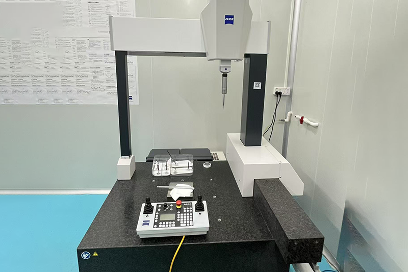
Detecting and Measuring Subsurface Damage
Effective SSD management requires both detection capability and process control. YISHUN Optical employs multiple characterization techniques:
Chemical Etching (Etch Pit Density)
The most common SSD detection method involves chemically etching the polished surface to reveal subsurface defects as etch pits. Etchants selectively attack damaged regions, allowing defect density quantification via microscopy.
| Material | Common Etchant | Etch Time |
|---|---|---|
| Fused Silica | HF/NH4F buffered | 30-120 seconds |
| BK7 Glass | HF diluted | 10-60 seconds |
| Sapphire | H3PO4 at 150°C | 5-30 minutes |
| SiC | KOH molten | 2-10 minutes |
| Germanium | HNO3/HF mixture | 30-120 seconds |
Etch pit density (EPD) measurement provides quantitative SSD assessment, with industry standards typically specifying maximum allowable EPD values for specific applications.
Acoustic Microscopy (SAM/C-SAM)
Scanning Acoustic Microscopy detects subsurface delaminations, voids, and cracks through ultrasonic beam reflection variations. Particularly effective for multilayer optics and coated components where chemical etching would damage functional layers.
Transmission Electron Microscopy (TEM)
Cross-sectional TEM analysis provides atomic-scale resolution of subsurface damage structure. While destructive and time-consuming, TEM reveals detailed damage morphology including dislocation networks, crack configurations, and amorphized layers.
Scatterometer Measurements
Total Integrating Scatter (TIS) measurements detect light scattered by subsurface imperfections, providing non-destructive SSD estimation through correlations with known damage levels.
Birefringence Mapping
Stress-induced birefringence measurements using polarimetry can indicate residual stress distribution in subsurface layers, indirectly assessing processing damage.
SSD Mitigation Strategies and Process Optimization
Preventing SSD introduction and removing damage from prior operations requires systematic process optimization:
Optimized Grit Progression
The most fundamental SSD mitigation strategy involves carefully controlled grit progression that removes previously damaged material while introducing minimal new damage:
Recommended Grit Progression Sequence:
- Coarse Grind (60-120 mesh): Initial shaping, accepts deep SSD
- Fine Grind (240-400 mesh): Reduces damage depth to 3-8μm
- Superfine Grind (600-1200 mesh): Minimizes damage to <2μm
- Pre-Polish (3-6μm diamond): Transition step
- Final Polish (1μm or finer): Removes remaining SSD and achieves surface finish
Each transition must remove material depth equal to at least 3× the maximum damage depth from the previous operation.
Process Parameter Optimization
| Parameter | Effect on SSD | Recommended Practice |
|---|---|---|
| Grinding Depth of Cut | Deeper cuts = more damage | Minimize depth; multiple light passes |
| Wheel Grade/Hardness | Harder wheels = more damage | Match wheel to material hardness |
| Coolant Flow | Insufficient cooling = thermal damage | Maintain continuous, adequate flow |
| Abrasive Size Distribution | Wide distribution = variable damage | Use narrow-grading abrasives |
| Polishing Pad Selection | Hard pads = potential damage | Match pad hardness to material |
Stress-Relief Annealing
Intermediate or final annealing processes relieve residual stress introduced during grinding and polishing. Thermal annealing schedules must consider material-specific properties:
- Fused Silica: 1100°C for 2-4 hours, controlled cooling
- BK7 Glass: 500-550°C for 1-2 hours
- Sapphire: 1600°C for 4-6 hours
Annealing reduces birefringence and improves mechanical stability but adds processing time and cost.
MRF for SSD Reduction
Magnetorheological finishing can effectively remove grinding-induced SSD while minimizing new damage introduction. MRF’s sub-aperture removal mechanism and controlled pressure distribution reduce mechanical stress on the subsurface layer.
Final Etch or Ion Beam Finishing
For ultra-low SSD requirements, final material removal via:
- Chemical etching: Selectively removes damaged surface layer
- Ion beam figuring (IBF): Non-contact material removal without mechanical damage
- Plasma-assisted chemical etching (PACE): Chemically enhanced material removal
These techniques achieve SSD-free surfaces but require careful process control to avoid introducing different defect types.
Application-Specific SSD Requirements
SSD tolerance varies significantly by application:
| Application | Max SSD Depth | Detection Requirement |
|---|---|---|
| High-Power Laser Optics | <0.5μm | Mandatory, etch + scatter |
| UV Lithography Optics | <0.1μm | Mandatory, multiple methods |
| Precision Metrology | <2μm | Recommended |
| Imaging Systems | <5μm | Standard inspection |
| 一般光学组件 | <10μm | Basic verification |
| Consumer Optics | <20μm | Industry standard |
YISHUN Optical’s SSD Management Approach
YISHUN Optical’s precision optical manufacturing integrates comprehensive SSD management:
Process Design:
- Optimized grit progression based on material and specification
- Proprietary process parameters minimizing damage introduction
- Stress-relief protocols for critical applications
Quality Assurance:
- Statistical process control with SSD checkpoints
- Multiple detection capabilities (etching, scatterometry, birefringence)
- Complete documentation of processing history
Certification:
- ISO 9001:2015 certified quality management system
- Customer-specific requirements compliance
- Full traceability from raw material to finished component
Conclusion
Subsurface damage represents a critical quality parameter that surface roughness specifications alone cannot capture. Understanding SSD origins, detection methods, and mitigation strategies enables informed process selection and supplier evaluation for precision optical components.
For high-power laser applications, UV optics, and mission-critical systems, SSD management is not optional—it’s essential for reliable component performance.
YISHUN Optical’s comprehensive approach to subsurface damage optical polishing combines decades of process expertise with advanced detection capabilities. Our engineering team evaluates each application’s SSD requirements and implements appropriate mitigation strategies.
Contact info@yishunoptical.com or visit yishunoptical.com to discuss your precision optical requirements with our technical team.
YISHUN Optical delivers ISO 9001:2015 certified precision optical components with comprehensive SSD management. Our 20+ years of experience serving Apple, BYD, Philips, and other industry leaders ensures consistent quality for the most demanding applications.
Frequently Asked Questions
What causes subsurface damage in optical polishing?
Subsurface damage originates primarily from grinding operations, where abrasive particles create micro-cracks and plastic deformation extending into the material. Polishing processes can either remove this damage or introduce new SSD if process parameters (pressure, pad hardness, abrasive size) are inappropriate. Material removal at any stage involves mechanical stress that may create subsurface defects.
How do you detect subsurface damage?
Common detection methods include chemical etching (revealing damage as etch pits), scanning acoustic microscopy (detecting cracks and delaminations), scatterometry (measuring light scatter from subsurface defects), and birefringence mapping (detecting residual stress). The selection depends on material, defect type, and inspection requirements.
Does subsurface damage affect laser damage threshold?
Yes, significantly. Subsurface damage directly correlates with reduced laser-induced damage threshold (LIDT). Micro-cracks and stress concentrations create localized energy hot spots where laser damage initiates at power levels well below the intrinsic material LIDT. Components with minimal SSD consistently achieve 2-5× higher LIDT values.
How deep does subsurface damage extend?
Typical SSD depths range from 0.5μm to 50μm depending on processing. Coarse grinding introduces damage 20-50μm deep, while fine grinding keeps depths below 3μm. Proper polishing and stress-relief processes can reduce subsurface damage to <0.5μm for the most demanding applications.
Can subsurface damage be completely eliminated?
Complete elimination is challenging but achievable for critical applications through a combination of optimized grit progression, stress-relief annealing, and final finishing techniques like ion beam figuring or chemical etching. For most applications, SSD is reduced to acceptable levels rather than entirely eliminated.
What is the relationship between surface roughness and subsurface damage?
Surface roughness and subsurface damage are related but distinct quality parameters. A smooth surface (Ra <1nm) can still contain significant subsurface damage, while properly processed surfaces can achieve low SSD with slightly higher roughness. Both parameters must be independently specified and verified for critical optical components.
How does SSD affect optical component durability?
Subsurface damage compromises mechanical durability by introducing stress concentrations and crack initiation sites. Under thermal cycling, vibration, or mechanical loading, SSD can propagate and cause component failure. For aerospace and defense applications, SSD management is essential for meeting lifetime and reliability requirements.