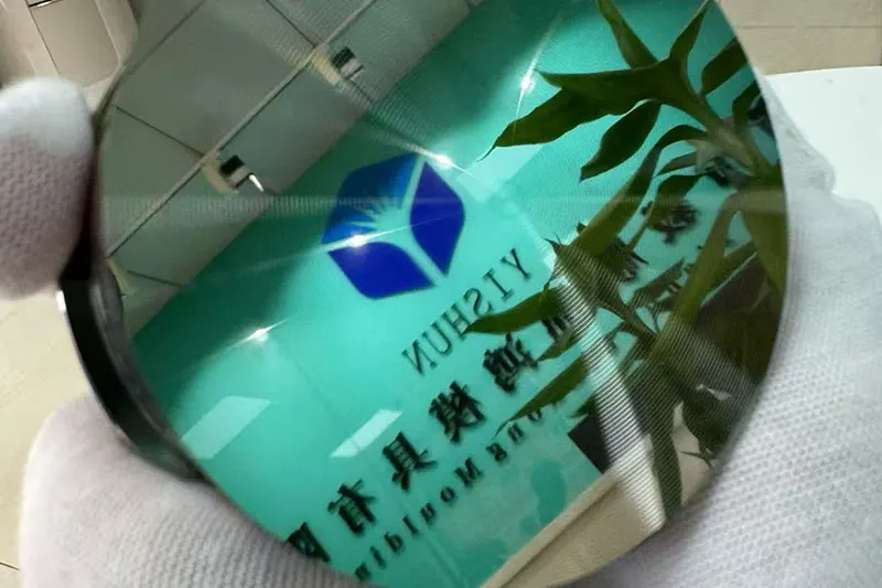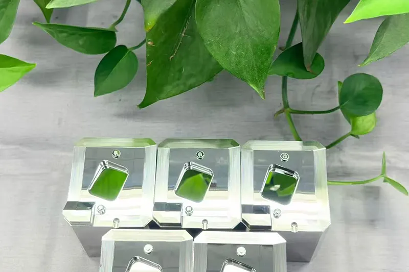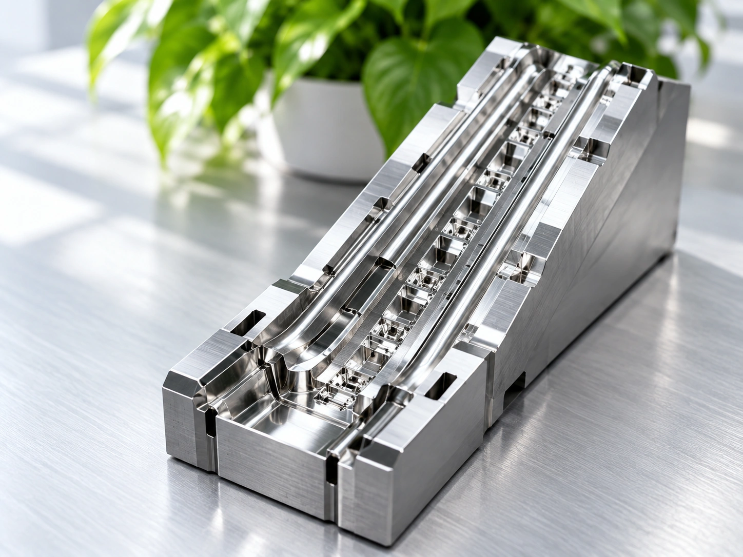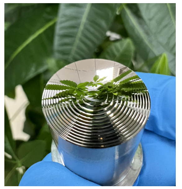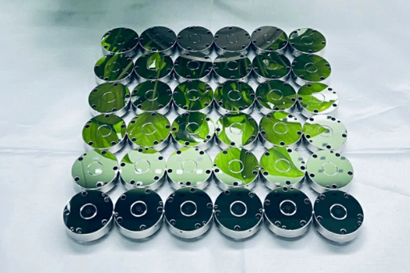
Subsurface damage in optical components refers to hidden microcracks, residual stress, embedded abrasive particles, voids, and structural defects beneath the visible surface of an optic. It is often introduced during sawing, grinding, lapping, or polishing, and it can reduce optical performance even when the surface looks smooth.
For precision optics, surface roughness alone is not enough to judge quality. A component may appear visually polished while still containing damaged material below the surface. This hidden damage can increase light scatter, absorption, coating failure risk, and laser-induced damage, especially in high-power laser, imaging, semiconductor, and medical optical systems. Research on optical glass also shows that low surface roughness does not necessarily mean the absence of subsurface damage.
For manufacturers, the key question is not only “Can the part be polished?” but also “Has the previous grinding or lapping damage been fully removed?” This is where a controlled optical polishing and lapping process becomes critical.
If your optical components require tight flatness, low roughness, and reliable surface integrity, professional optical polishing and lapping services can help control the full finishing process from material removal to final inspection.
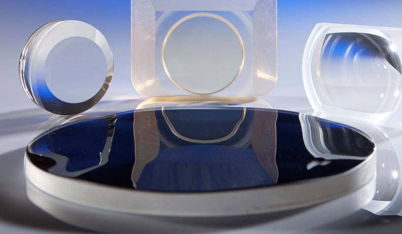
What Is Subsurface Damage in Optical Components?
Subsurface damage, often abbreviated as SSD, is damage located below the top surface layer of an optical component. It is usually invisible under normal visual inspection. In optical glass and brittle optical materials, SSD may include:
- Median cracks extending downward into the material
- Lateral cracks running parallel to the surface
- Residual stress caused by mechanical force
- Embedded polishing compound or abrasive particles
- Microvoids, pits, or fracture networks
- Chemically altered or redeposited surface layers
The most important feature of subsurface damage is that it can remain hidden after polishing, even when the optical surface appears clean, glossy, and smooth.
This is especially important for optical glass, fused silica, sapphire, quartz, ceramics, and other hard brittle materials. During mechanical processing, abrasive particles remove material by micro-cutting, plowing, and fracture. If the polishing step only smooths the top layer but does not remove the deeper damaged zone, the component may still fail in demanding optical applications.
Industry references note that grinding and polishing can leave subsurface damage from about 0.1 μm to tens of microns below the polishing redeposition layer, depending on material and process conditions.
Why Subsurface Damage Matters for Optical Performance
Subsurface damage is not just a cosmetic issue. It can directly affect how light interacts with the component.
In high-performance optical systems, even small defects below the surface may cause measurable performance loss. For example, microcracks and embedded contaminants can increase absorption and scatter. In laser optics, these defects may create localized heating and reduce laser-induced damage threshold.
Main risks caused by subsurface damage
| Risk | How SSD Affects the Component | Typical Impact |
|---|---|---|
| Light scatter | Microcracks and pits disturb light transmission or reflection | Lower image contrast, stray light |
| Absorption | Contaminants and damaged zones absorb optical energy | Local heating, reduced throughput |
| Coating failure | Defects under coatings act as weak points | Peeling, cracking, poor adhesion |
| Lower laser damage threshold | Damage sites concentrate energy | Premature failure in laser systems |
| Mechanical weakness | Subsurface cracks may grow under stress | Lower reliability and fatigue resistance |
| Poor repeatability | Hidden damage varies between batches | Unstable product performance |
For laser optics, semiconductor optics, imaging optics, and precision molds, controlling subsurface damage is essential for both optical performance and long-term reliability.
What Causes Subsurface Damage During Optical Manufacturing?
Subsurface damage is usually introduced during earlier mechanical processing steps. The more aggressive the material removal process, the deeper the potential damage zone.
1. Cutting and sawing
Initial blank preparation can introduce deep cracks, chipped edges, and stress zones. These defects are often much deeper than those created by fine grinding or polishing. If later process steps do not remove enough material, early-stage damage may remain in the final part.
2. Grinding
Grinding removes material efficiently but can create brittle fracture beneath the surface. Coarse grinding wheels or aggressive feed rates may increase SSD depth.
Important grinding-related factors include:
- Abrasive grit size
- Wheel bond type
- Cutting depth
- Feed rate
- Coolant condition
- Material hardness and fracture toughness
3. Lapping
Lapping is commonly used to improve flatness and dimensional accuracy. However, loose abrasive particles can still create microcracks if the pressure, abrasive size, or process time is not properly controlled.
4. Polishing
Polishing is used to reduce roughness and improve optical surface quality. However, polishing does not automatically remove all subsurface damage. In some cases, polishing can create a redeposition or chemically modified surface layer that visually hides underlying defects. Edmund Optics notes that an ineffective polishing process may hide damage under the Beilby layer rather than remove deep subsurface defects.
5. Poor process transition
A common mistake is moving from coarse grinding directly to fine polishing without enough intermediate material removal. Each step must remove the damage created by the previous step before moving to a finer abrasive.
A correct optical finishing process removes material progressively, so each finer step eliminates the deeper damage left by the previous rougher step.
Surface Roughness vs. Subsurface Damage: Why They Are Not the Same
Many buyers focus heavily on roughness values such as Ra, RMS, or scratch-dig. These are important, but they do not fully describe subsurface integrity.
Surface roughness describes the topography of the visible or measurable surface. Subsurface damage describes defects beneath that surface.
A part can have:
- Low roughness but hidden cracks
- Good visual polish but residual stress
- Acceptable flatness but embedded abrasive contamination
- Smooth surface but reduced laser damage resistance
This is why precision optical components should be evaluated not only by surface finish but also by process history and application risk.
Comparison table
| Item | Surface Roughness | Subsurface Damage |
|---|---|---|
| Location | Top surface | Beneath the surface |
| Visibility | Measurable by profilometer or interferometer | Often hidden |
| Common unit | Ra, RMS, nm, μm | Depth, morphology, defect density |
| Main cause | Final finishing quality | Grinding, lapping, polishing history |
| Main risk | Scatter, poor appearance, coating issues | Cracking, laser damage, coating failure |
| Can polishing improve it? | Usually yes | Only if enough material is removed |
How to Detect Subsurface Damage in Optical Components
Subsurface damage detection can be destructive or non-destructive. The right method depends on component value, material, required precision, and whether the part is a prototype or production item.
Common SSD inspection methods
| Method | Type | What It Reveals | Advantages | Limitations |
|---|---|---|---|---|
| Chemical etching | Destructive | Crack networks and damaged zones | Useful for process validation | Alters the part |
| Cross-section microscopy | Destructive | Damage depth and morphology | Direct observation | Requires sample cutting |
| Taper polishing / MRF spot | Semi-destructive | SSD depth through controlled removal | High precision for development | Not always suitable for finished parts |
| SEM inspection | Destructive or sample-based | Fine crack morphology | High resolution | Requires sample preparation |
| Optical microscopy | Often destructive after etching | Surface and near-surface defects | Accessible and practical | Limited depth information |
| Raman spectroscopy | Non-destructive | Stress or structural changes | Useful for certain materials | Requires expertise |
| X-ray diffraction | Non-destructive | Residual stress and crystal damage | Useful for crystalline materials | Not universal for all optics |
| Laser scattering methods | Non-destructive | Scatter related to defects | Relevant to optical performance | Interpretation can be complex |
Academic reviews describe destructive methods such as taper sectioning, cross-sectioning, and chemical etching, as well as non-destructive methods based on Raman response and X-ray diffraction.
For production projects, not every component needs destructive SSD testing. However, SSD analysis is very useful during process development, new material qualification, high-power laser optics manufacturing, and failure analysis.
How to Eliminate or Minimize Subsurface Damage
In practice, “eliminating” subsurface damage means removing the damaged layer from previous processes and reducing newly introduced damage to an acceptable level for the application. Absolute zero damage is difficult to prove in all materials, but a well-controlled process can greatly reduce SSD risk.
1. Start with the right material preparation
Good SSD control begins before polishing. If sawing or grinding creates deep damage, the polishing stage must remove more material, increasing time and cost.
Material preparation should consider:
- Cutting method
- Edge chipping control
- Grinding depth
- Coolant and slurry cleanliness
- Material brittleness
- Allowance for later removal
2. Use controlled lapping to improve flatness
Lapping is often used to improve flatness before final polishing. The goal is to remove earlier deep damage while avoiding excessive new cracks.
Key lapping controls include:
- Abrasive particle size
- Lapping pressure
- Plate condition
- Slurry concentration
- Process time
- Cleaning between abrasive stages
For high-precision optical parts, a supplier with experience in precision optical lapping and polishing can help define the correct sequence rather than relying on a single final polishing step.
3. Reduce abrasive size gradually
Abrasive progression is one of the most important SSD control strategies. Moving from coarse to fine abrasives in proper steps reduces the risk of leaving deep damage behind.
A simplified process may look like this:
| Process Stage | Purpose | SSD Control Focus |
|---|---|---|
| Rough grinding | Shape generation | Avoid excessive crack depth |
| Fine grinding | Reduce previous damage | Improve surface before lapping |
| Lapping | Improve flatness and remove damage | Control pressure and abrasive size |
| Pre-polishing | Reduce roughness | Remove lapping marks |
| Final polishing | Achieve optical finish | Minimize redeposition and contamination |
| Cleaning and inspection | Verify quality | Prevent particles and residue |
4. Remove enough material at each stage
Every process step should remove enough material to eliminate the deepest damage from the previous step. If insufficient material is removed, the final surface may look polished while older cracks remain underneath.
The safest polishing strategy is not simply to make the surface shiny, but to remove the full damaged layer created by earlier grinding and lapping steps.
5. Control polishing chemistry and slurry contamination
Polishing slurry can improve material removal and surface finish, but contamination creates risk. Embedded abrasive particles or polishing residues may become trapped near the surface.
Good practice includes:
- Using clean slurry
- Filtering or replacing slurry when needed
- Avoiding cross-contamination between abrasive sizes
- Cleaning parts thoroughly between process stages
- Matching polishing chemistry to the optical material
6. Use advanced finishing methods when required
For demanding optics, conventional polishing may not be enough. Depending on material and application, advanced finishing may include:
- Magnetorheological finishing
- Chemical mechanical polishing
- Ion beam figuring or ion beam etching
- Fluid jet polishing
- Superpolishing
- Precision pitch polishing
Scientific literature has discussed surface treatments such as magnetorheological finishing and ion beam etching as methods for minimizing or eliminating SSD in optical substrates.
7. Verify with the right inspection method
A process should be validated by measurement, not assumption. For standard optics, surface roughness, flatness, visual inspection, and dimensional checks may be sufficient. For high-power laser or mission-critical optics, SSD-specific testing may be needed.
Engineering Factors That Influence SSD Depth
Subsurface damage depth depends on both the material and the process. The following factors should be reviewed before choosing an optical polishing supplier.
| Factor | Why It Matters | Engineering Recommendation |
|---|---|---|
| Material hardness | Harder materials may require more aggressive removal | Use material-specific abrasive strategy |
| Fracture toughness | Brittle materials crack more easily | Reduce mechanical stress during lapping |
| Abrasive size | Larger particles can create deeper cracks | Use gradual abrasive reduction |
| Processing pressure | High pressure increases crack risk | Optimize load and contact conditions |
| Process time | Too short may leave old damage; too long may affect geometry | Balance removal and precision |
| Slurry condition | Contaminated slurry can scratch or embed particles | Maintain clean process control |
| Final application | Laser optics require stricter SSD control | Define inspection based on risk |
Common Mistakes When Trying to Remove Subsurface Damage
Mistake 1: Judging quality only by appearance
A mirror-like surface does not automatically mean low SSD. The surface may be visually smooth while hidden cracks remain underneath.
Mistake 2: Skipping intermediate lapping or polishing steps
Trying to save time by skipping abrasive stages may increase the risk of retained damage.
Mistake 3: Using the same process for every material
Sapphire, quartz, fused silica, optical glass, silicon carbide, and ceramics respond differently to grinding and polishing. A process that works for one material may not work for another.
Mistake 4: Ignoring the final application
A component for decorative appearance does not need the same SSD control as a component for a high-power laser system. The polishing process should match the application.
Mistake 5: Not discussing inspection requirements early
SSD control should be discussed before production, not after parts fail inspection. Buyers should define roughness, flatness, scratch-dig, coating, and laser or imaging requirements in advance.
How to Choose an Optical Polishing and Lapping Supplier
When sourcing optical polishing or lapping services, the supplier should understand both surface quality and subsurface integrity.
A qualified supplier should be able to discuss:
- Material type and brittleness
- Required flatness and parallelism
- Surface roughness target
- Scratch-dig or cosmetic requirements
- Coating requirements
- Laser wavelength and power density if applicable
- Batch consistency
- Inspection and measurement methods
- Process control from rough lapping to final polishing
YISHUN Optical’s optical polishing and lapping services page states capabilities including nano-level surface finishing, tight dimensional tolerance, flatness control, and experience with optical glass, ceramics, metals, plastics, sapphire, silicon carbide, and quartz.
For buyers, the practical point is simple: do not only ask for a low Ra value. Ask how the supplier controls the full process chain that creates, reduces, and verifies surface and subsurface quality.
What Information Should You Provide Before Requesting a Quote?
To help an optical polishing supplier evaluate SSD risk and process feasibility, prepare the following information:
| Information | Why It Helps |
|---|---|
| Material | Determines polishing method and abrasive selection |
| Part dimensions | Affects fixturing, flatness, and handling |
| Initial condition | Shows how much damage may need to be removed |
| Required roughness | Defines final polishing target |
| Required flatness | Determines lapping and measurement strategy |
| Coating requirement | SSD can affect coating adhesion and durability |
| Optical application | Laser, imaging, medical, semiconductor, or mold use |
| Quantity | Affects process planning and cost |
| Inspection standard | Prevents disagreement after production |
The more clearly these requirements are defined, the easier it is to design a reliable finishing process.
FAQ: Subsurface Damage in Optical Components
1. What causes subsurface damage in optical components?
Subsurface damage is usually caused by sawing, grinding, lapping, or polishing. Coarse abrasives, high pressure, poor slurry control, and insufficient material removal between process steps can leave microcracks and residual stress beneath the surface.
2. Can optical polishing completely remove subsurface damage?
Optical polishing can remove subsurface damage if enough material is removed to eliminate the damaged layer from previous processing. However, simply making the surface smooth or shiny does not guarantee that all deeper damage has been removed.
3. How do you know if an optical component has subsurface damage?
Subsurface damage can be detected using methods such as chemical etching, cross-section microscopy, taper polishing, MRF spot testing, SEM, Raman spectroscopy, X-ray diffraction, or laser scattering methods. The best method depends on the material and application.
4. Is low surface roughness enough to prove there is no subsurface damage?
No. Low surface roughness does not always prove that subsurface damage is absent. A surface can be smooth while still containing hidden cracks, residual stress, or embedded contaminants below the top layer.
5. Why is subsurface damage important for laser optics?
In laser optics, subsurface defects can increase absorption, scatter, and localized heating. This may reduce laser-induced damage threshold and increase the risk of optical failure under high-power laser exposure.
6. What is the difference between lapping and polishing for SSD removal?
Lapping is mainly used to improve flatness and remove material in a controlled way, while polishing is used to reduce roughness and achieve optical surface quality. Both may be needed to remove earlier process damage and prepare the final optical surface.
7. How can buyers reduce SSD risk when sourcing optical parts?
Buyers should provide material, application, roughness, flatness, coating, and inspection requirements before production. They should also work with a supplier experienced in controlled optical polishing and lapping rather than choosing only by price.
Conclusion
Subsurface damage in optical components is one of the most important hidden risks in precision optics manufacturing. It may not be visible on the surface, but it can affect scatter, absorption, coating reliability, laser damage resistance, and long-term mechanical stability.
The most effective way to eliminate subsurface damage is to control the full manufacturing chain: material preparation, grinding, lapping, polishing, cleaning, and inspection.
For demanding optical components, a reliable polishing partner should not only achieve low roughness and tight flatness but also understand how earlier process steps influence hidden subsurface integrity.
If your project involves optical glass, quartz, sapphire, ceramics, precision molds, laser components, or high-performance optical parts, YISHUN Optical can support your project with professional optical polishing and lapping services tailored to your surface quality and precision requirements.