Optical surface quality is not defined by a single number. Engineers normally need to control several different types of surface error, including localized defects, microscopic texture, and overall geometric form.
Scratch-dig describes discrete surface imperfections, surface roughness describes microscopic height variations, and flatness describes how far the overall surface departs from an ideal plane.
These parameters are related to optical manufacturing quality, but they are not interchangeable. A component can have low roughness but still contain a visible scratch. It can have excellent scratch-dig quality but poor flatness. It can also be highly flat while retaining microscopic texture that increases optical scatter.
Understanding these distinctions helps engineers specify polished components correctly, select appropriate inspection methods, and avoid unnecessary manufacturing cost.
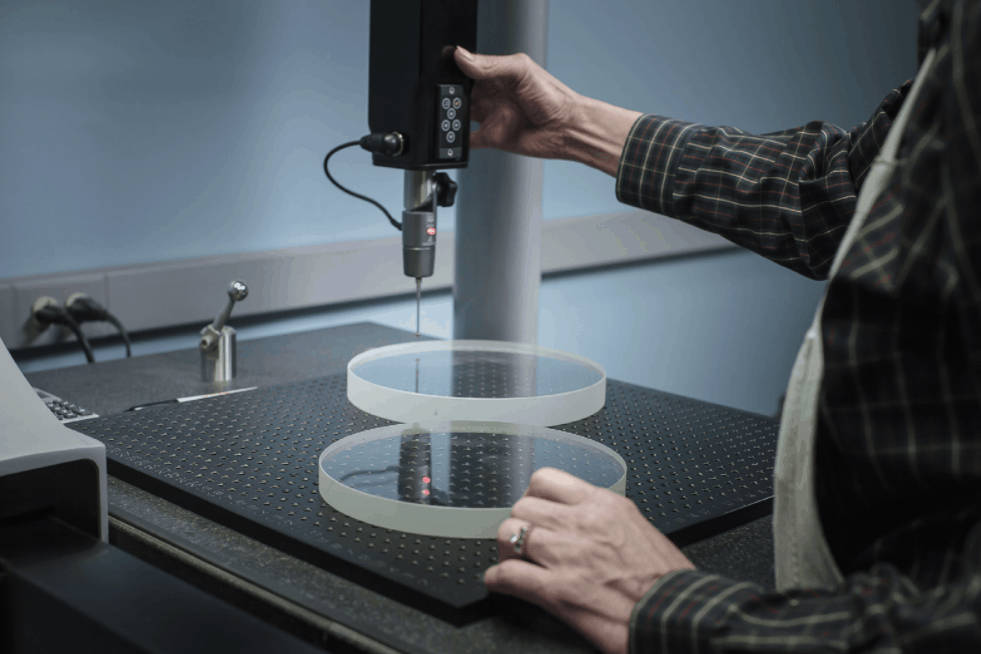
What Does Optical Surface Quality Mean?
The phrase “optical surface quality” is used in two ways.
In a broad engineering sense, it may refer to the complete condition of an optical surface, including:
- Scratches and pits;
- Surface roughness;
- Waviness;
- Flatness or surface form;
- Edge chips;
- Coating defects;
- Contamination;
- Subsurface damage.
In some purchasing documents, however, “surface quality” is used more narrowly to mean scratch-dig or other visible surface imperfections.
This difference in terminology can create confusion. A drawing that states only “optical-quality surface” does not provide enough information for manufacturing or inspection. The drawing should identify the specific parameters, limits, inspection standard, test area, and measurement conditions.
ISO separates these surface characteristics into different parts of the ISO 10110 drawing standard. ISO 10110-7 addresses surface imperfections, while ISO 10110-8 addresses surface texture. Surface form tolerances, including flat-surface form, are addressed separately under ISO 10110-5. (ISO)
Scratch-Dig, Roughness and Flatness at a Glance
| Parameter | What it describes | Typical scale | Common inspection method | Main functional concern |
| Scratch-dig | Localized visible defects such as scratches and pits | Individual defects | Controlled visual comparison or specified defect measurement method | Scatter, appearance, coating defects and local damage |
| Surface roughness | Fine microscopic texture across a sampling area | High spatial frequency | Optical profilometer, coherence scanning interferometer or other surface profiler | Scatter, reflection, transmission, coating and contact behavior |
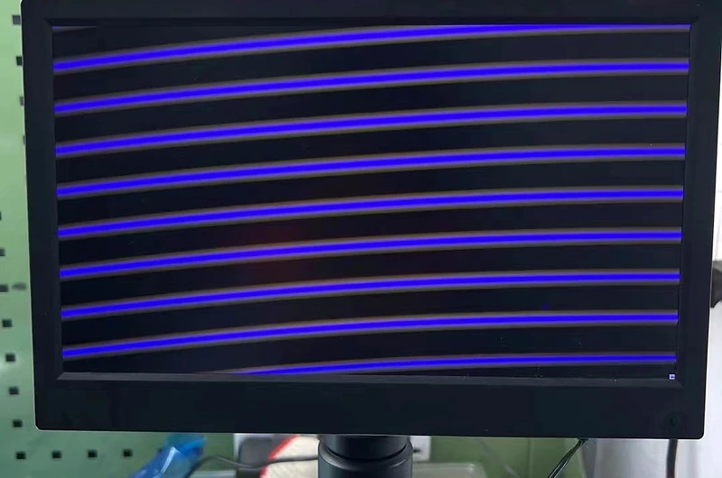
| Flatness | Overall departure from an ideal plane | Low spatial frequency or full aperture | Fizeau interferometer, optical flat or form-measuring system | Wavefront distortion, alignment, bonding and sealing |
| Waviness | Repeating or intermediate-scale surface variation | Mid-spatial frequency | Optical profiler or interferometric analysis | Stray light, image contrast and beam modulation |
| Edge quality | Chips, bevel damage and edge defects | Localized edge region | Visual or dimensional inspection | Handling reliability, cracking and assembly |
A complete optical surface specification often requires separate limits for surface imperfections, surface roughness and surface form.
What Is Scratch-Dig?
Scratch-dig is a commonly used method for specifying visible or localized imperfections on optical surfaces.
A scratch is generally an elongated surface imperfection. A dig is generally a localized pit, indentation or defect with a more compact shape.
Examples of imperfections covered by surface-quality inspection may include:
- Polishing scratches;
- Pits or digs;
- Sleeks;
- Edge chips;
- Coating blemishes;
- Fractures;
- Local stains or process marks, depending on the agreed standard.
ISO 10110-7:2017 defines requirements for indicating the acceptable level of surface imperfections within a defined test region. It includes localized imperfections, long scratches and edge chips. (ISO)
What Do Numbers Such as 60-40 Mean?
A scratch-dig designation is normally written as two numbers, such as:
- 60-40;
- 40-20;
- 20-10;
- 10-5.
The first number refers to the scratch requirement, while the second refers to the dig requirement.
Within the same inspection system, lower numbers generally represent a stricter limit on allowable imperfections. However, these numbers should not be interpreted without identifying the standard.
In legacy MIL-style inspection, scratch evaluation is based primarily on appearance comparison against reference standards rather than a straightforward measurement of physical scratch width. Dig requirements are treated differently and are more closely related to defect size.
For this reason, stating “40-20 scratch-dig” without naming the governing standard, illumination conditions, test area and inspection method can lead to disagreement between customer and supplier.
The Optics and Electro-Optics Standards Council notes that scratch-dig specifications are among the most frequently misunderstood and ambiguously interpreted optical specifications. It also distinguishes inspection practices associated with MIL, ANSI and ISO systems. (OEOSC)
Scratch-Dig Is Not a Roughness Measurement
A polished surface may have extremely low average roughness but still contain one isolated scratch caused by:
- Abrasive contamination;
- Improper cleaning;
- Handling;
- Fixture contact;
- Residual particles;
- Damage during coating or packaging.
Conversely, a surface may contain no obvious scratches but still have excessive microscopic roughness.
Scratch-dig evaluates discrete imperfections; it does not describe the average microscopic texture of the entire surface.
What Is Optical Surface Roughness?
Optical surface roughness describes fine-scale height variations across a measured area or profile.
Every manufactured surface contains variations at different spatial scales. ZYGO separates these broadly into form, waviness and roughness, with roughness representing the fine texture generated by manufacturing processes such as grinding, lapping and polishing. (Zygo)
ISO 10110-8:2019 defines rules for indicating optical surface texture and identifies roughness with high-spatial-frequency surface errors and waviness with mid-spatial-frequency errors. (ISO)
Common Roughness Parameters
| Parameter | Meaning | Important consideration |
| Ra | Arithmetic average of absolute profile-height deviations | Common in mechanical drawings but depends on sampling and filtering |
| Rq or RMS | Root-mean-square value of height deviations | More sensitive to larger peaks and valleys than Ra |
| Sa | Areal arithmetic mean height measured over a surface area | Three-dimensional equivalent of a profile-based average |
| Sq | Areal root-mean-square surface height | Common in 3D optical surface analysis |
| Peak-to-valley | Difference between the highest and lowest measured points | Strongly affected by isolated defects and measurement area |
Ra and Rq should not be treated as automatically interchangeable. Their relationship depends on the surface-height distribution, measurement bandwidth, filtering method and sampling conditions.
A roughness report should therefore state more than one numerical result. It should also identify:
- Measurement instrument;
- Objective or magnification;
- Scan size;
- Sampling interval;
- Filter or cutoff;
- Number and location of measurements;
- Whether the result is profile-based or area-based;
- Whether scratches or isolated defects were removed from the analysis.
Why Surface Roughness Matters
Excessive roughness can affect:
- Optical scatter;
- Reflective performance;
- Transmission;
- Coating adhesion and uniformity;
- Laser-system losses;
- Bonding or sealing surfaces;
- Friction and contact behavior;
- Cleanability.
The importance of a roughness value depends on the wavelength, optical configuration, coating, angle of incidence and application. A roughness requirement suitable for a mechanical contact surface may not be sufficient for a precision optical mirror or laser component.
How Is Optical Roughness Measured?
Common methods include:
- Coherence scanning interferometry;
- White-light interferometry;
- Phase-shifting interferometry for suitable surfaces;
- Confocal optical profiling;
- Atomic force microscopy for very small areas;
- Stylus profilometry for compatible materials and applications.
Non-contact optical profilers can measure three-dimensional surface topography without physically touching the polished surface. ZYGO describes coherence scanning interferometry as a method capable of measuring smooth, rough, flat, sloped and stepped surfaces, depending on instrument configuration. (Zygo)
The measurement method must match the expected roughness range, material reflectivity, surface slope and required sampling area.
What Is Optical Flatness?
Flatness describes the deviation of a nominally flat surface from an ideal reference plane.
It is a surface-form requirement rather than a microscopic texture requirement. A surface can be highly polished and visually clean but still be curved, warped, twisted or locally deformed.
Flatness is especially important for:
- Optical windows;
- Mirrors;
- Wafers;
- Precision substrates;
- Bonding surfaces;
- Sealing interfaces;
- Reference flats;
- Semiconductor components;
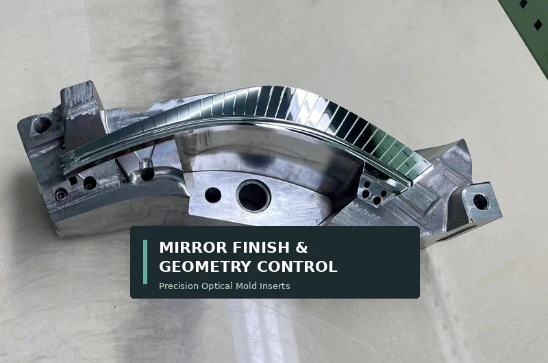
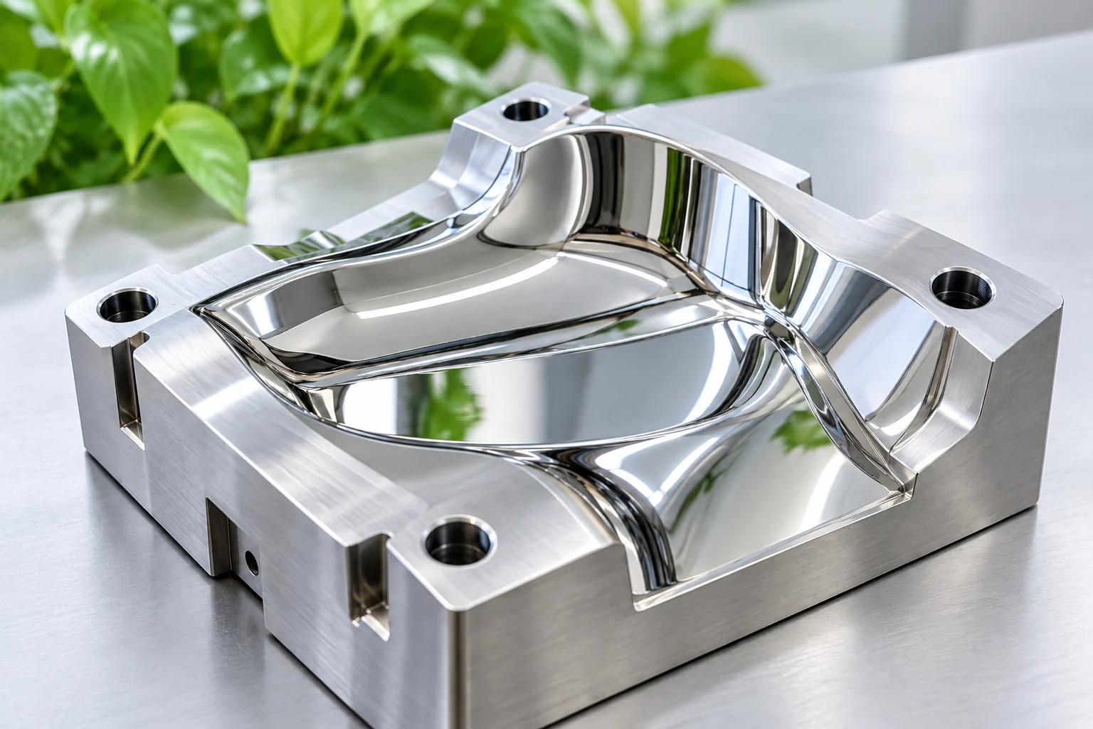
- Optical mold inserts.
Flatness in Micrometers and Fractions of a Wavelength
Flatness may be specified in dimensional units, such as:
- Micrometers;
- Nanometers;
- Peak-to-valley deviation;
- RMS surface-form error.
It may also be specified as a fraction of an optical wavelength:
- 1λ;
- λ/2;
- λ/4;
- λ/10;
- λ/20.
A wavelength-based specification is incomplete unless the reference wavelength is defined. A λ/10 requirement at one wavelength represents a different physical height tolerance from λ/10 at another wavelength.
The drawing or purchase specification should state:
- Test wavelength;
- Clear aperture or test region;
- Peak-to-valley or RMS evaluation;
- Whether power or curvature is removed;
- Surface orientation;
- Measurement setup;
- Reference surface requirements.
ZYGO notes that laser interferometry is commonly used to measure flatness and surface form by comparing a test surface with a calibrated optical reference. (Zygo)
Flatness Is Not the Same as Parallelism
Flatness applies to one individual surface.
Parallelism describes the angular or geometric relationship between two opposite surfaces. A component can have two individually flat surfaces that are not parallel to one another.
For an optical window or substrate, engineers may need to specify:
- Surface flatness;
- Parallelism or wedge;
- Thickness;
- Thickness variation;
- Transmitted wavefront error.
These requirements should not be replaced by one general “flatness” value.
The Spatial-Frequency Difference
One useful way to understand optical surface quality is to separate surface errors by spatial frequency.
| Surface characteristic | Spatial scale | Example |
| Surface form | Low spatial frequency | Overall bow, curvature or astigmatic deformation |
| Waviness | Mid spatial frequency | Periodic polishing marks or tool-path structure |
| Roughness | High spatial frequency | Microscopic peaks and valleys |
| Scratch-dig | Localized, non-periodic defects | Individual scratch, pit or chip |
The boundaries between form, waviness and roughness depend on the filtering and measurement setup. The same raw surface data may produce different reported values if the evaluation bandwidth or cutoff is changed.
This is why suppliers and customers should agree on both the numerical tolerance and the data-processing method.
Can a Surface Pass One Requirement and Fail Another?
Yes. Each parameter evaluates a different property.
Example 1: Low Roughness but Poor Scratch-Dig
A surface may measure Ra 1 nm across several clean sampling areas but contain one visible handling scratch elsewhere. It may pass the roughness requirement while failing the scratch-dig requirement.
Example 2: Good Scratch-Dig but Poor Flatness
A component may look visually clean and free from scratches but have excessive bow across the aperture. It may pass cosmetic inspection but distort a transmitted or reflected wavefront.
Example 3: Good Flatness but Excessive Roughness
A lapped component may have accurate overall geometry but retain a matte or microscopically rough surface. It may pass flatness inspection but require further polishing.
Example 4: Good Average Roughness but Unacceptable Waviness
A measured surface may show a low Ra value while retaining periodic tool marks. These mid-spatial-frequency errors may still affect imaging contrast, stray light or beam quality.
No single optical surface-quality value can confirm the complete performance of a polished component.
How Optical Polishing and Lapping Affect These Parameters
Lapping and polishing perform related but different functions.
Lapping is commonly used to:
- Improve flatness;
- Correct parallelism;
- Control thickness;
- Remove grinding damage;
- Establish a stable geometry before final polishing.
Polishing is commonly used to:
- Reduce microscopic roughness;
- Remove fine process marks;
- Improve optical clarity or reflectivity;
- Reduce localized surface defects;
- Prepare a surface for coating or final inspection.
However, polishing does not automatically improve every parameter. Excessive or uneven polishing may reduce roughness while degrading flatness or creating edge roll-off. Contaminated polishing media may create new scratches even when the general surface finish improves.
Projects that require both geometry control and low roughness may therefore need a combined optical polishing and lapping process.
How to Specify Optical Surface Quality Correctly
A practical drawing or RFQ should define each relevant requirement separately.
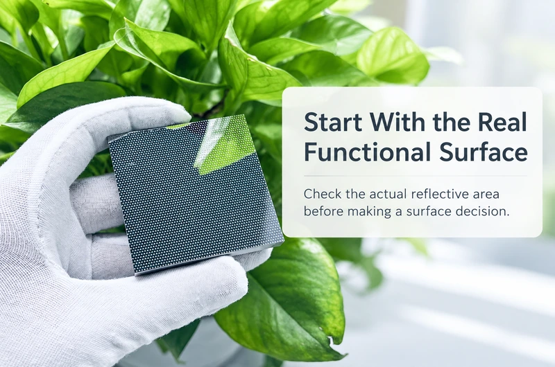
1. Define the Functional Surface
Identify:
- Clear aperture;
- Coated area;
- Bonding area;
- Sealing area;
- Non-critical edge zone;
- Cosmetic-only region.
The strictest specification does not always need to apply across the entire component.
2. Identify the Governing Standard
State whether the surface-imperfection requirement follows:
- ISO 10110-7;
- A specific ANSI/OEOSC method;
- A legacy MIL-style requirement;
- A mutually agreed customer specification.
Do not mix the notation from one standard with the inspection procedure from another.
3. Define the Roughness Metric
Specify:
- Ra, Rq, Sa or Sq;
- Maximum allowable value;
- Measurement area;
- Filter or cutoff;
- Number of locations;
- Instrument or approved equivalent method.
4. Define Flatness Completely
Specify:
- Maximum PV or RMS error;
- Physical units or wavelength fraction;
- Test wavelength;
- Clear aperture;
- Whether curvature or power is removed;
- Required interferogram or measurement report.
5. Define Inspection Documentation
The supplier may be asked to provide:
- Scratch-dig inspection record;
- Roughness map or profile;
- Interferogram;
- Flatness PV and RMS values;
- Instrument identification;
- Calibration status;
- Part and drawing revision;
- Inspection date;
- Lot or serial-number traceability.
Example Optical Surface Specification Table
| Requirement | Example format | Additional information required |
| Surface imperfections | Scratch-dig 40-20 | Governing standard, clear aperture and inspection conditions |
| Surface roughness | Ra ≤ specified value | Scan size, cutoff, instrument and measurement locations |
| Surface flatness | ≤ λ/4 PV | Test wavelength, aperture and data-removal settings |
| Parallelism | Maximum angular deviation | Datum surfaces and measurement method |
| Edge chips | Maximum allowable size | Edge zone and quantity limit |
| Coating quality | Visual or defect requirement | Coated area, illumination and acceptance standard |
The numerical values in this table are illustrative formats, not universal recommendations. Actual requirements should be based on the optical and mechanical function of the part.
Common Specification Mistakes
Using “Optical Polish” Without Numerical Requirements
“Optical polish” may indicate a general manufacturing intent, but it does not define acceptable roughness, flatness or defects.
Treating Scratch-Dig as Physical Scratch Width
In appearance-based scratch systems, the scratch designation should not automatically be interpreted as a direct measured width.
Omitting the Inspection Standard
The same numerical notation may be interpreted differently under different standards or internal inspection procedures.
Specifying λ/10 Without a Wavelength
A wavelength fraction must include the reference wavelength to define a physical tolerance.
Reporting Roughness Without Measurement Bandwidth
A roughness value depends on measurement area, resolution and filtering. Results from two instruments may not be directly comparable.
Applying the Tightest Requirement Everywhere
Non-functional edge regions may not require the same specification as the clear optical aperture. Unnecessary restrictions can increase polishing time and rejection risk.
Assuming Better Numbers Always Improve Performance
A tighter surface requirement may add cost without improving the actual system if another error source dominates performance.
How to Evaluate an Optical Polishing Supplier
A supplier should be able to explain how each requirement will be manufactured and verified.
Ask the following questions:
- Which process controls flatness before final polishing?
- How will scratch-dig be inspected?
- Which standard and comparison method will be used?
- Which instrument measures roughness?
- What scan size and filter will be reported?
- How will flatness be measured?
- What test wavelength and aperture will be used?
- Can the supplier provide representative inspection reports?
- How are polished parts cleaned and packaged?
- How are results controlled between prototype and production batches?
A supplier should not claim that one inspection method proves all aspects of optical surface quality.
For components requiring geometry correction and final surface finishing, YISHUN Optical provides precision optical polishing and lapping services for custom optical and technical components.
According to its published service information, YISHUN lists surface roughness capability down to Ra 1 nm, flatness capability down to 0.1 μm and dimensional tolerances down to ±0.5 μm for suitable projects. These values should be evaluated according to material, geometry, part size, measurement area and inspection method rather than applied universally to every component. (YISHUN Optical)
Engineering teams can review YISHUN Optical and submit drawings, material information and inspection requirements for project-specific evaluation.
FAQ
What is optical surface quality?
Optical surface quality describes the condition of a finished optical surface. Depending on context, it may include scratches, digs, roughness, waviness, flatness, edge defects and coating imperfections. Each characteristic should be specified separately.
What is the difference between scratch-dig and surface roughness?
Scratch-dig controls localized imperfections such as individual scratches and pits. Surface roughness measures microscopic height variation across a defined area or profile. A surface can pass one requirement and fail the other.
What does 60-40 scratch-dig mean?
In a 60-40 designation, the first number refers to the scratch requirement and the second to the dig requirement. Lower numbers generally indicate stricter limits within the same standard, but the governing inspection standard must be stated.
Is optical flatness the same as surface roughness?
No. Flatness describes overall deviation from an ideal plane, while roughness describes fine microscopic texture. Flatness is usually evaluated across a larger aperture, whereas roughness is measured over a smaller sampling area.
How is optical surface roughness measured?
Optical surface roughness is commonly measured with an optical profilometer, coherence scanning interferometer, white-light interferometer or another suitable surface-metrology system. The report should state the measurement area, filter and roughness parameter.
How is optical flatness measured?
Optical flatness is commonly measured using an interferometer or optical flat. The result may be reported in micrometers, nanometers or fractions of a wavelength. The test wavelength and aperture should be defined.
Is Ra the same as RMS roughness?
No. Ra is the arithmetic average of absolute height deviations, while RMS or Rq is the root-mean-square height deviation. They may produce different values and should not be substituted without agreement.
Can polishing remove all scratch-dig defects?
Polishing can remove many fine scratches and pits, but deep defects may require additional grinding or lapping. Some defects may be too deep to remove without changing dimensions or surface form.
Which optical surface-quality standard should I use?
The appropriate standard depends on the customer, industry and inspection system. ISO 10110 is widely used for optical drawings, while ANSI/OEOSC and legacy MIL-style scratch-dig systems are also used. The standard and inspection method should be agreed before production.
What information should I send with an optical polishing RFQ?
Provide the material, drawing, dimensions, quantity, clear aperture, scratch-dig requirement, roughness metric, flatness tolerance, test wavelength, edge requirement, coating needs and required inspection reports.
Conclusion
Scratch-dig, roughness and flatness describe three different aspects of optical surface quality.
Scratch-dig controls localized imperfections. Roughness controls microscopic texture. Flatness controls the overall geometric form of a nominally flat surface.
The most reliable optical specification defines each relevant parameter separately and includes the governing standard, test region, measurement method and acceptance criteria.
For custom components requiring controlled surface form and finish, engineers can discuss their specifications with YISHUN Optical and evaluate an appropriate custom optical polishing solution based on the part’s material, geometry and application.