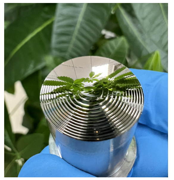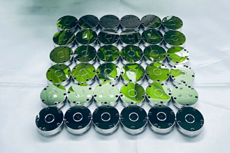
When optical component specifications demand surface accuracies beyond λ/50—requiring figure corrections measured in single-digit nanometers and surface roughness approaching atomic dimensions—traditional polishing techniques reach their practical limits. Ion Beam Figuring (IBF) represents the ultimate deterministic surface finishing technology, using energetic ion bombardment to remove material without mechanical contact, achieving surface precisions unattainable through any other manufacturing method.
For engineers developing extreme-performance optical systems in lithography, astronomy, and laser physics, understanding IBF capabilities and limitations enables appropriate specification and supplier selection. YISHUN Optical’s IBF capabilities, integrated with complementary MRF and CMP processes, deliver optical components meeting the most demanding specifications for clients across high-reliability optical, semiconductor, and research institutions worldwide.
Key Takeaways
- IBF achieves material removal without mechanical contact, eliminating tool marks, subsurface damage, and process-induced surface degradation
- Nanometer-scale deterministic correction is achievable by controlling ion beam dwell time based on surface error mapping
- Surface roughness improvements to Ra < 0.1nm possible on suitable materials
- No tool wear effects since no physical tool contacts the surface
- Slower material removal rates compared to MRF or CMP; typically used for final correction after other finishing processes
Understanding Ion Beam Figuring Technology
The Physics of Ion-Surface Interaction
When accelerated ions collide with a solid surface, they transfer momentum to surface atoms through elastic collisions. This process, called sputtering, ejects atoms from the surface when the transferred energy exceeds the surface binding energy.
The sputtering yield (atoms removed per incident ion) depends on:
- Ion energy: Typically 0.5-2 keV for optical IBF applications
- Ion species: Argon, xenon, or reactive gases depending on material
- Incident angle: Maximum yield at 60-80° from surface normal
- Target material: Different materials have different sputtering thresholds
Key IBF Parameters
| Parameter | Typical Value | Effect on Process |
|---|---|---|
| Ion energy | 0.5-2.0 keV | Higher energy increases removal rate |
| Beam current | 1-50 mA | Current density determines removal rate |
| Beam diameter | 1-20 mm | Smaller beams enable finer correction |
| Incident angle | 0-90° from normal | Affects sputtering yield and micro-roughness |
| Working pressure | 10⁻⁴ to 10⁻³ Pa | Requires high vacuum environment |
IBF System Configuration
Vacuum Chamber and Ion Source
IBF systems operate in high vacuum environments:
- Oil-free pumping systems (turbomolecular + ion pumps) prevent hydrocarbon contamination
- Ultra-high vacuum (UHV) components maintain cleanliness
- Sample manipulators provide precise positioning with sub-micrometer accuracy
- Multiple-axis motion enables raster scanning and dwell time control
Ion Source Technology
Kaufman-type ion sources are standard for optical IBF:
- Hot cathode design: Tungsten filament or LaB₆ cathode
- Broad beam geometry: Uniform ion current across beam diameter
- Adjustable energy and current: Process optimization flexibility
- Long lifetime: Cathode replacement intervals of 500-2000 hours
Dwell Time Control System
The IBF correction process requires:
- High-precision surface mapping: Zygo interferometer or similar system
- Removal function characterization: Measure material removal rate vs. beam position and time
- Dwell time calculation: Algorithm converts error map to scanning program
- Precision motion system: Executes dwell time distribution with < 0.1% accuracy
- Closed-loop verification: Post-IBF measurement confirms correction success
IBF Process Characteristics
Deterministic Material Removal
IBF exemplifies deterministic finishing—removal amount depends only on ion dose (beam current × dwell time), not on material properties or process artifacts:
Material Removal = Removal Rate × Dwell Time
This predictability enables precise figure corrections calculated from measured surface error maps. Unlike conventional polishing where tool wear, slurry degradation, and operator technique affect removal, IBF produces mathematically predictable material removal.
No Mechanical Contact
The absence of physical tool contact provides unique advantages:
- Zero subsurface damage: No mechanical deformation or micro-cracking
- No tool marks: No feed lines, tool tracks, or micro-scratches
- No edge effects: Material removal uniform at part edges
- No consumables wear: Removal function remains constant throughout processing
Material Compatibility
IBF works on virtually any material that can be sputtered:
| Material | IBF Compatible | Typical Performance |
|---|---|---|
| Fused silica | Yes | Excellent |
| BK7 glass | Yes | Excellent |
| Silicon | Yes | Very Good |
| Germanium | Yes | Very Good |
| Zerodur | Yes | Excellent |
| Aluminum | Yes (coated) | Requires protective coating |
| Nickel-phosphorus | Yes | Requires coating |
IBF vs. Alternative Finishing Technologies
Comparison with MRF
| Characteristic | IBF | MRF |
|---|---|---|
| Material removal mechanism | Sputtering | Fluid cell mechanical |
| Removal rate | 0.1-0.5 nm/min | 1-10 nm/min |
| Figure correction capability | λ/50-λ/100 | λ/20-λ/50 |
| Surface roughness | Ra < 0.1nm achievable | Ra 0.2-1nm |
| Edge effects | Minimal | Moderate |
| Process speed | Slow | Moderate |
| Capital cost | Very High | High |
Comparison with Conventional Polishing
- Conventional polishing produces Ra 0.5-5nm surfaces with figure corrections of λ/10
- MRF improves to Ra 0.2-1nm with λ/20 figure corrections
- IBF achieves Ra < 0.1nm with λ/50-λ/100 figure corrections
- Each technology represents an order-of-magnitude improvement over the previous
Applications Requiring IBF
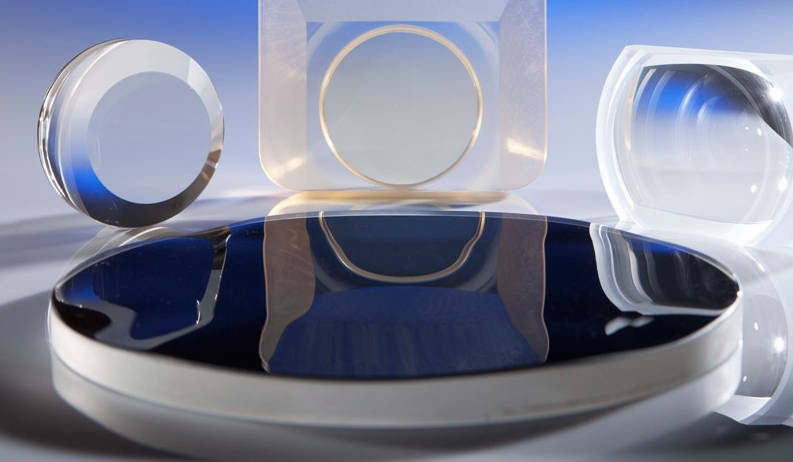
Semiconductor Lithography
EUV (extreme ultraviolet) lithography optics require unprecedented surface precision:
- Surface accuracy < 0.1nm RMS over meter-scale surfaces
- Mid-spatial-frequency control critical for image fidelity
- Low roughness minimizes flare and stray light
- IBF essential for achieving specifications unattainable otherwise
Astronomical Telescopes
high-precision and ground-based observatory mirrors require:
- Wavefront quality across large apertures
- Scatter reduction for contrast imaging (exoplanet detection)
- Stability under thermal and gravitational loading
- IBF corrections on aspheric segments for segmented mirror telescopes
Laser Gyroscopes
High-performance gyroscopes demand:
- Ultra-low scatter from mirror surfaces
- Dimensional stability over operational temperature range
- Minimal micro-roughness to reduce bias drift
- IBF polishing essential for navigation-grade performance
Research Lasers and FELs
Free-electron lasers and high-power research lasers:
- Highest LIDT (laser-induced damage threshold) requirements
- Sub-nanometer surface roughness for peak intensity control
- Wavefront quality for beam quality preservation
- IBF-processed optics provide necessary performance margin
IBF Process Integration
Typical Finishing Sequence
For highest-performance optics, YISHUN Optical employs optimized process sequences:
- Precision grinding: Generate near-net shape with < 1μm form accuracy
- Conventional polishing: Achieve Ra < 5nm and basic figure correction
- MRF processing: Correct figure to λ/20, improve MSFE
- CMP finishing (optional): Achieve Ra < 0.5nm on suitable materials
- IBF final correction: Final figure optimization to λ/50+
Each stage reduces remaining error, with IBF removing only nanometers of material for final optimization.
Process Monitoring
Throughout IBF processing:
- In-situ ion beam monitoring tracks removal rate stability
- Interferometric verification between processing iterations
- Surface roughness sampling using AFM or phase-shift microscopy
- Full-aperture measurement upon process completion
IBF Limitations and Considerations
Processing Time
IBF’s slow removal rate limits throughput:
- Typical removal rate: 0.1-0.5 nm/minute
- Full λ/10 correction (63nm) may require 2-8 hours
- High-value components justify extended processing times
- Not suitable for correcting gross errors; use upstream of IBF
Equipment Cost and Maintenance
- Capital investment significantly higher than MRF or CMP systems
- Vacuum system maintenance requires specialized expertise
- Ion source consumables (filaments, grids) require periodic replacement
- Process development requires experienced operators
Subsurface Damage Considerations
Unlike MRF, IBF can introduce subtle subsurface effects:
- Implantation zone: Ions penetrate 1-5nm below surface
- Lattice disorder: Crystalline materials may require annealing
- Residual stress: May affect long-term stability
- Process optimization minimizes these effects
YISHUN Optical’s IBF Capabilities
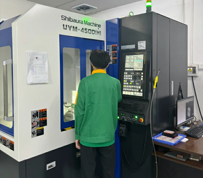
YISHUN Optical’s ion beam figuring capabilities include:
- IBF system with Kaufman ion source for precision figuring
- Sub-nanometer surface roughness achievable on optical glasses
- λ/50 figure correction capability with iterative processing
- Integration with MRF and CMP for complete finishing solutions
- In-house metrology for closed-loop process control
- ISO 9001:2015 certified quality system
Our combination of IBF, MRF, CMP, and conventional polishing processes enables selecting the optimal finishing approach for each component’s specific requirements.
Frequently Asked Questions
What is the minimum surface roughness achievable with IBF?
IBF can achieve Ra < 0.1nm (sub-angstrom) surface roughness on glass and crystalline materials. AFM measurements have verified surface roughness below 0.05nm RMS over measurement bandwidths appropriate for optical scatter prediction.
Does IBF damage the optical surface?
IBF produces no mechanical subsurface damage since no physical contact occurs. However, ion implantation creates a modified layer 1-5nm deep. For most applications, this effect is negligible; for highest LIDT requirements, post-IBF annealing may be specified.
How long does IBF processing take?
IBF processing time depends on correction magnitude. A typical λ/20 correction (3nm over aperture) might require 30-60 minutes of active processing. Corrections larger than λ/10 may require multiple hours. Process planning accounts for this limitation by using upstream processes for coarse corrections.
What materials cannot be processed by IBF?
IBF works on nearly all optical materials through sputtering. However, some materials with very high sputter thresholds or those that decompose under ion bombardment may present challenges. Organic materials and certain plastics cannot be IBF-processed. Our engineering team evaluates material compatibility for each application.
Is IBF cost-effective for production volumes?
IBF is typically reserved for high-value precision optics rather than high-volume production due to slow processing rates. For production quantities, MRF alone often provides sufficient surface quality at higher throughput. YISHUN recommends IBF when specifications require λ/50+ figure accuracy or Ra < 0.2nm surface roughness.
How does IBF compare to IBF polishing?
IBF (Ion Beam Figuring) focuses on figure correction—removing material at specific locations to improve surface shape. IBF polishing (sometimes called IBP or ion beam polishing) focuses on micro-smoothing—improving surface roughness without significant figure change. Both use similar ion beam technology but serve different purposes.
Conclusion
Ion Beam Figuring represents the ultimate deterministic surface finishing technology, capable of achieving figure corrections measured in nanometers and surface roughness approaching atomic dimensions. While the technology’s slow removal rate and high cost limit application to highest-precision requirements, IBF enables optical systems that would otherwise be impossible to manufacture.
YISHUN Optical’s integration of IBF with complementary finishing technologies—MRF, CMP, and conventional polishing—provides complete manufacturing capability for optics requiring the ultimate in surface precision. Combined with our ISO 9001:2015 certified quality system and precision metrology capabilities, we deliver optical components meeting the most demanding specifications for research, high-reliability optical, and semiconductor applications.
Need extreme-precision optical surfaces? Contact YISHUN Optical’s engineering team at info@yishunoptical.com or visit yishunoptical.com to discuss how IBF can achieve your surface precision requirements.