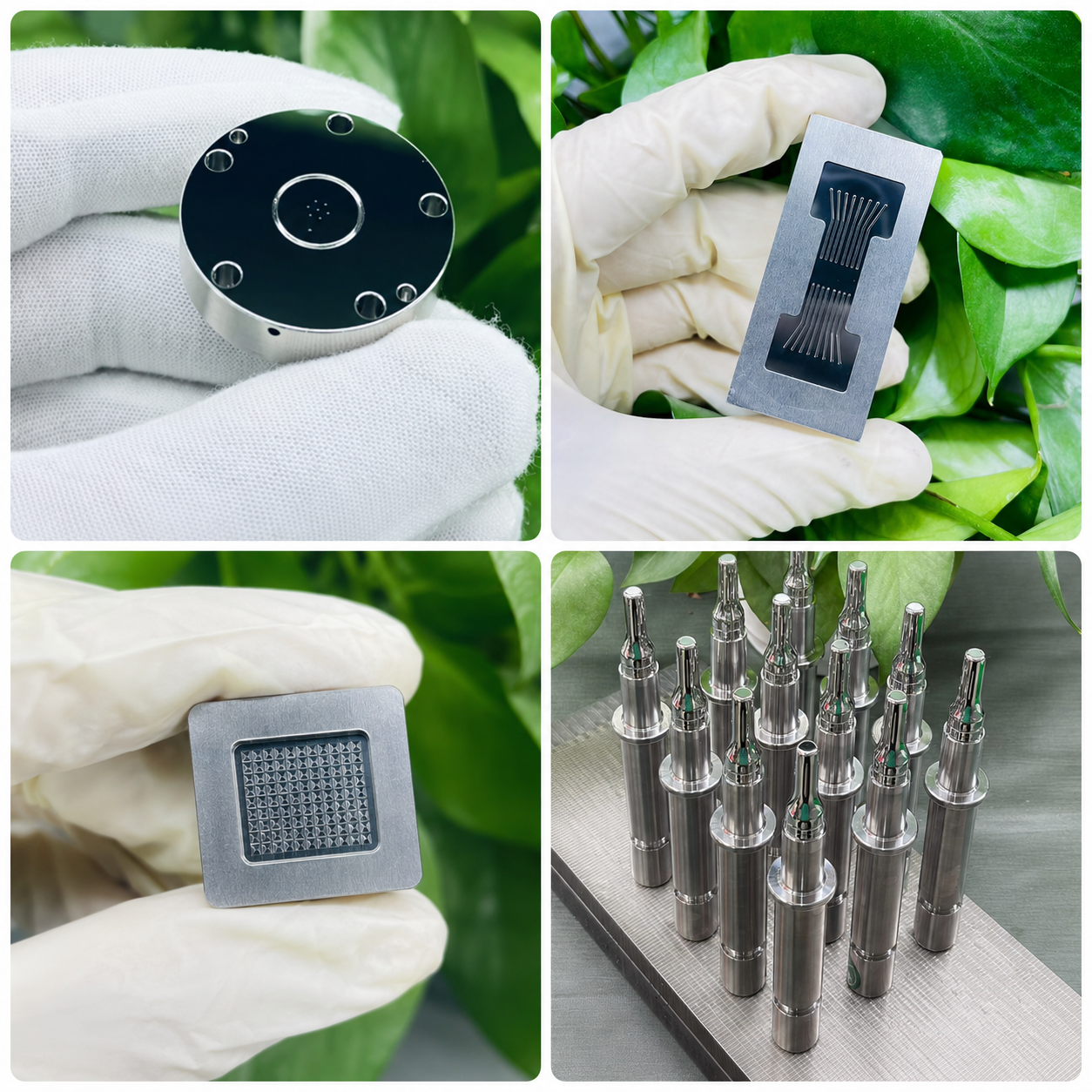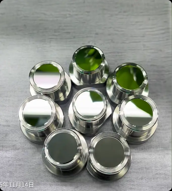
Lithography mold processing requires achieving sub-micron tolerances while maintaining contamination-free surfaces essential for advanced semiconductor manufacturing. Yishun Optical delivers cleanroom optical mold fabrication through specialized ultra-precision machining in Class 10 environments, with 4 Toshiba UVM machining centers achieving PV≤0.15μm and surface finishes reaching Ra≤0.005μm. This technical guide examines the precision requirements, process technologies, and quality assurance protocols that enable lithography mold manufacturing at the nanoscale.
Modern photolithography systems demand optical molds with surface figure errors below λ/20 (measured at 632.8nm), placing extraordinary requirements on manufacturing processes. Yishun Optical’s 20+ years of experience in precision mold manufacturing, combined with 2 Moore single-point diamond turning lathes (Ra≤2nm), positions the company as a leading provider of lithography mold processing services.

The Critical Role of Optical Molds in Photolithography
Optical Mold Function and Requirements
Optical molds in photolithography serve as precision templates for transferring circuit patterns onto semiconductor wafers. These molds, also called photomasks or reticles, contain the geometric information that defines device structures at nanometer scales.
The surface quality of lithography molds directly influences pattern transfer fidelity and ultimately determines device performance. Sub-surface damage introduced during machining creates fatal defects that propagate through the entire wafer during exposure.
Cleanroom optical mold manufacturing prevents particle contamination that would compromise pattern integrity. Even a single particle on the mold surface can cause a defect that renders an entire chip unusable, making contamination control as critical as dimensional precision.
Yishun Optical’s expertise in lithography mold processing supports semiconductor manufacturers requiring surfaces that meet SEMI standards while maintaining nanometer-level figure accuracy.
Precision Engineering for Sub-Micron Tolerances
Machine Tool Requirements
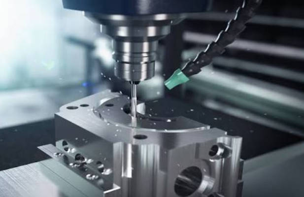
Achieving sub-micron tolerances demands machine tools with exceptional stiffness, thermal stability, and positioning accuracy. Yishun Optical’s 4 Toshiba UVM ultra-precision machining centers provide positioning accuracy suitable for lithography mold applications, with PV (Peak-to-Valley) values of 0.15μm or better.
Hydrostatic bearing systems eliminate vibration and friction that compromise surface quality in conventional machining. Air bearings provide sub-micron motion accuracy while maintaining the thermal stability required for long-duration machining operations.
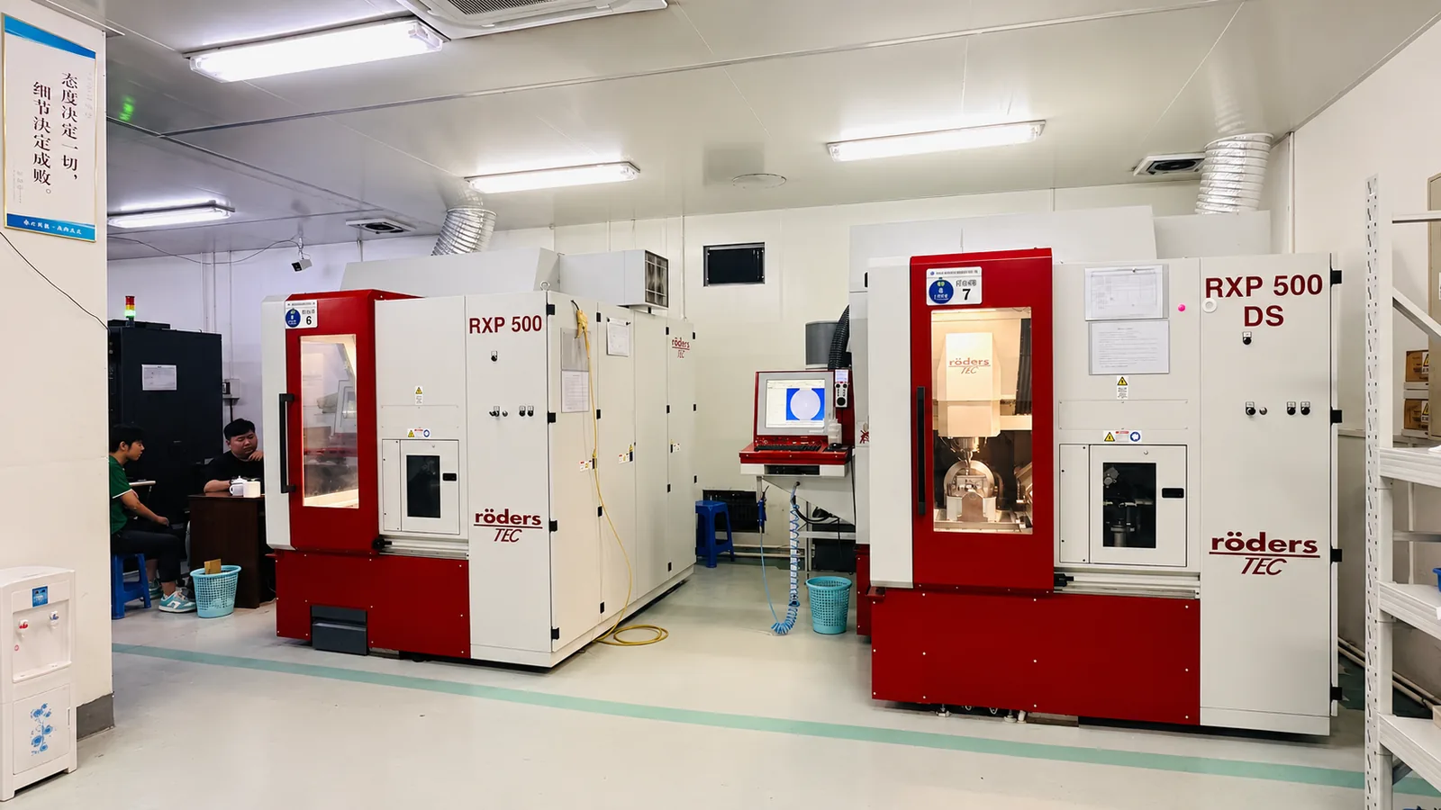
Five-axis machining capability enables complex mold geometries that optimize lithography performance. The Röders RXP500DS and Roku Roku machines in Yishun Optical’s facility deliver the multi-axis accuracy required for advanced photolithography applications.
Environmental Control in Ultra-Precision Machining
Temperature stability proves essential for maintaining machining accuracy at the nanometer scale. Yishun Optical maintains machining environments at 20±0.5°C with humidity controlled to 45±5% RH, preventing thermal expansion from introducing dimensional errors.
Vibration isolation systems protect delicate machining operations from environmental disturbances. Foundation isolation and active vibration control enable the precision necessary for lithography mold fabrication.
The integration of environmental control with ultra-precision machine tools enables Yishun Optical to achieve tolerances that would be impossible under conventional manufacturing conditions.
Surface Generation Techniques
Diamond Turning of Optical Molds
Single-point diamond turning (SPDT) produces deterministic surfaces with nanometer-level finishes directly from the machine tool. Yishun Optical’s 2 Moore single-point diamond turning lathes achieve Ra≤2nm surfaces without requiring subsequent polishing operations.
Diamond turning excels with aluminum and copper alloys commonly used in lithography mold substrates. The process generates optical-quality surfaces in a single setup, eliminating multiple grinding and polishing operations that accumulate positioning errors.
Tool geometry and cutting parameters require careful optimization to achieve defect-free surfaces. Yishun Optical’s process engineering team has developed proprietary techniques that minimize tool wear while maximizing surface quality.
Precision Grinding for Hard Materials
Hard materials including stainless steel, tool steel, and ceramic substrates require precision grinding rather than diamond turning. Yishun Optical employs advanced grinding techniques with wheel specifications optimized for specific material combinations.
Creep-feed grinding removes material efficiently while maintaining form accuracy across large mold surfaces. The process generates surfaces suitable for subsequent polishing operations that achieve final figure specifications.
Residual stress management during grinding prevents distortion that could compromise final mold flatness. Yishun Optical’s heat treatment and stress-relief processes ensure dimensional stability throughout the manufacturing workflow.
Cleanroom Optical Mold Manufacturing Protocols
Contamination Prevention Strategies
Cleanroom optical mold manufacturing begins with material preparation in controlled environments. All materials undergo particle removal and cleanliness verification before entering the production workflow.
Yishun Optical’s Class 10 cleanroom maintains airborne particle counts below 10 particles per cubic foot at 0.5μm, matching semiconductor fab requirements. Personnel protocols, including specialized cleanroom garments, prevent human-generated contamination from entering the manufacturing environment.
Tool changes, measurement operations, and inspection procedures all occur within the controlled cleanroom space. This integrated approach ensures that finished molds emerge with contamination levels suitable for semiconductor applications.
Handling and Storage Procedures
Proper handling preserves cleanroom surfaces throughout the manufacturing process and subsequent shipment. Yishun Optical employs precision handling fixtures that prevent surface contact and particle generation during transport.
Protective packaging maintains cleanliness during storage and shipment. Desiccated containers prevent moisture adsorption that could affect dimensional stability or promote corrosion.
Complete documentation tracks handling history from raw material through delivery, enabling traceability that semiconductor customers require.
Surface Quality Enhancement
Pitch Polishing for Optical Surfaces
Pitch polishing employs sub-material flow characteristics to achieve figure correction without introducing sub-surface damage. This process enables nanometer-level figure improvements while preserving the subsurface integrity essential for lithography applications.
Yishun Optical’s pitch polishing operations achieve surface figure errors below λ/20, meeting the most demanding lithography requirements. Process parameters including polish pitch composition, temperature, and dwell time are optimized for specific mold geometries.
The flexibility of pitch polishing enables correction of form errors across large areas while maintaining surface quality in critical regions. This adaptability proves essential for lithography molds with complex pattern layouts.
Computer-Controlled Optical Surfacing (CCOS)
CCOS technologies apply deterministic material removal based on surface metrology feedback. Yishun Optical’s computer-controlled polishing systems map surface errors and calculate optimal tool paths that converge toward target specifications.
The iterative CCOS process achieves figure accuracies beyond conventional polishing techniques. Multiple measurement-polation cycles refine surface quality until specifications are satisfied.
Integrated interferometric metrology enables real-time surface characterization throughout the CCOS process. This feedback-driven approach maximizes efficiency while ensuring specification compliance.
Metrology and Quality Assurance
Interferometric Surface Measurement
Phase-shifting interferometry provides nanometer-resolution surface metrology essential for lithography mold verification. Yishun Optical maintains calibrated interferometers traceable to national standards, ensuring measurement confidence.
Surface figure measurements at multiple wavelengths enable characterization of both mid-spatial and high-spatial frequency errors. This comprehensive analysis identifies issues that could affect lithography performance.
Power spectral density (PSD) analysis characterizes surface errors across all spatial frequencies, providing insights that support process optimization. Statistical process control using PSD metrics ensures consistent quality across production batches.
Surface Roughness Characterization
White light interferometry measures surface roughness at nanometer resolution across large measurement areas. Yishun Optical’s metrology laboratory characterizes surface finish across representative sample locations, verifying Ra≤0.005μm specifications.
Atomic force microscopy (AFM) provides nanoscale surface analysis for critical regions requiring ultra-smooth finishes. These measurements complement broader interferometric surveys to ensure comprehensive surface quality verification.
Sub-surface damage assessment using chemical etching techniques reveals subsurface integrity that could affect long-term lithography performance. Yishun Optical’s quality protocols verify absence of damage that could compromise mold reliability.
Material Considerations for Lithography Molds
Substrate Material Selection
Material selection for lithography molds balances thermal stability, machinability, and durability requirements. Fused silica offers exceptional thermal stability but requires specialized grinding techniques. Ultra-low expansion (ULE) glass-ceramics provide dimensional stability across temperature variations.
Metal substrates including aluminum alloys enable efficient diamond turning while providing adequate durability for moderate-volume production applications. Yishun Optical’s material expertise guides customer selections based on specific application requirements.
Surface coatings including chromium, aluminum, and specialty materials enhance reflectivity and durability for transmission or reflection lithography applications. Coating processes require careful optimization to preserve underlying figure accuracy.
Coatings and Surface Enhancement
Reflective coatings for reticle substrates require ultra-smooth base surfaces that preserve pattern edge quality. Yishun Optical’s precision polishing creates substrates optimized for coating adhesion and reflectivity.
Anti-reflection coatings for transmission masks require precise thickness control achieved through ion beam sputtering or similar advanced deposition techniques. Surface preparation preceding coating deposition critically influences coating performance.
Advanced Lithography Mold Applications
Extreme Ultraviolet (EUV) Lithography
EUV lithography imposes unprecedented requirements on mask blank quality and pattern fidelity. Reflective multilayer coatings require atomically smooth surfaces that preserve coating uniformity across the entire mask area.
Yishun Optical’s precision manufacturing capabilities extend to EUV-compatible substrates requiring surface figure below 0.3nm PV. These requirements represent the ultimate challenge in precision mold manufacturing.
Multi-Patterning and Advanced Nodes
Multi-patterning lithography schemes require mask sets with exceptional pattern placement accuracy. Yishun Optical’s precision machining and metrology capabilities enable mask blanks that support advanced node manufacturing.
The coordination between multiple masks in multi-patterning schemes demands tight uniformity specifications across all mask sets. Yishun Optical’s process controls ensure consistency that enables successful multi-patterning integration.
Industry Standards and Compliance
SEMI Standards for Lithography Molds
SEMI standards establish specifications and test methods that ensure mask quality consistent across the semiconductor industry. Yishun Optical’s quality management system incorporates SEMI requirements into manufacturing protocols.
Cleanliness verification following SEMI guidelines confirms contamination levels suitable for intended lithography applications. Particle counting and defect inspection verify surface quality that prevents yield-limiting defects.
Dimensional verification protocols ensure pattern placement accuracy that supports overlay requirements for advanced nodes. Yishun Optical’s metrology capabilities enable characterization at the nanometer scale required for cutting-edge lithography.

Partnering with Yishun Optical
Engineering Collaboration
Yishun Optical’s engineering team engages with customers during design phases to optimize lithography mold manufacturability. Design for Manufacturing (DFM) reviews identify potential issues before production, reducing development time and cost.
Material selection assistance, process development, and qualification testing all benefit from Yishun Optical’s 20+ years of experience in precision optical manufacturing. The company’s technical expertise supports customers at every stage from concept through production.
Production Capability and Capacity
Four Toshiba UVM machining centers and two Moore diamond turning lathes provide capacity for production volumes while maintaining the precision essential for lithography applications. Yishun Optical’s facility supports both prototype development and volume production.
The ABB 6-axis robotic polishing system ensures repeatable surface quality across production batches. This automated capability complements skilled operator expertise to deliver consistent results.
Conclusion
Lithography mold processing demands exceptional precision across every manufacturing dimension—from environmental control and machine tool capability through surface generation and metrology verification. Sub-micron tolerances require integrated approaches that address all factors influencing achievable accuracy.
Yishun Optical combines advanced manufacturing capabilities with cleanroom infrastructure and rigorous quality systems to deliver cleanroom optical mold products that meet semiconductor industry requirements. The company’s Class 10 cleanroom, ultra-precision machining equipment, and experienced engineering team provide the foundation for lithography mold manufacturing excellence.
For lithography mold processing requiring sub-micron tolerances and contamination-free surfaces, partner with Yishun Optical. Our commitment to precision excellence and customer collaboration supports your most demanding photolithography applications.
Email: yishun158@163.com | Phone: +86-755-82594863 | Website: https://yishunoptical.com/
FAQ
Q1: What surface figure accuracy can Yishun Optical achieve for lithography molds?
A: Yishun Optical achieves surface figure errors below λ/20 (approximately 30nm at 632.8nm) through computer-controlled optical surfacing. Our precision machining and polishing capabilities enable PV values of 0.15μm or better on machined surfaces.
Q2: What cleanroom classification does Yishun Optical maintain for optical mold manufacturing?
A: Yishun Optical operates Class 10 cleanroom facilities that meet semiconductor manufacturing contamination standards. This controlled environment ensures particle counts below 10 particles per cubic foot at 0.5μm throughout the manufacturing process.
Q3: What surface roughness can be achieved on lithography molds?
A: Our 2 Moore single-point diamond turning lathes achieve Ra≤2nm directly from machining. Subsequent pitch polishing can further improve surface finish to Ra≤0.005μm for the most demanding lithography applications.
Q4: What materials does Yishun Optical work with for lithography molds?
A: We process fused silica, ultra-low expansion glass-ceramics, aluminum alloys, and specialty materials based on application requirements. Our engineering team assists with material selection to optimize performance for specific lithography technologies.
Q5: How does Yishun Optical verify sub-micron tolerances?
A: We employ phase-shifting interferometry for surface figure measurement, white light interferometry for roughness characterization, and coordinate measuring machines for dimensional verification. All metrology equipment is calibrated traceable to national standards.
Q6: Does Yishun Optical provide prototype and volume production services?
A: Yes, our manufacturing capabilities support both prototype development and high-volume production. Four Toshiba UVM machining centers and automated polishing systems provide capacity for diverse production requirements.
Q7: What certifications does Yishun Optical hold for quality assurance?
A: Yishun Optical maintains ISO 9001 (Quality Management), ISO 14001 (Environmental Management), and Apple Gold Supplier certification. The company is designated as a National High-Tech Enterprise and Specialized & New Enterprise (2024).