In the realm of high-performance optics, the difference between a successful mission and a total system failure often comes down to a few nanometers. Whether you are developing a deep-space telescope, a high-energy laser system, or a cutting-edge medical imaging device, the quality of your optical surfaces is paramount.
However, “quality” in the optical industry is not a subjective term. It is a rigorously measured, mathematically defined set of parameters. For anyone seeking optical polishing services, understanding how these surfaces are measured—a field known as metrology—is the key to ensuring you receive components that perform exactly as designed.
This guide is designed to walk you through the complex world of optical metrology, explaining the tools, the math, and the standards that define world-class surface quality.
I. The Invisible Difference: Why Metrology Matters
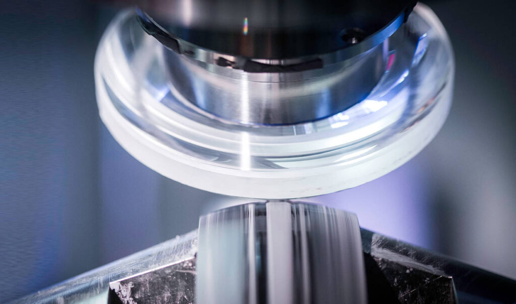
When you hold a polished lens or mirror, it may look perfect to the naked eye. However, at the microscopic and atomic levels, that surface is a landscape of peaks, valleys, and textures. Metrology in optical polishing is the essential process of quantifying surface deviations to ensure they fall within the specific tolerances required for a given application.
Without precise metrology, polishing is merely guesswork. Advanced optical polishing services rely on a constant feedback loop: the optician polishes the surface, the metrologist measures the result, and the data informs the next step of the polishing process. This cycle continues until the “Surface Figure” and “Surface Roughness” meet the customer’s specifications.
The Role of Metrology in Quality Assurance
For a customer, metrology is your insurance policy. It provides the empirical proof that the component you paid for will function in your optical assembly. A professional service provider should always provide a comprehensive metrology report (often called a Certificate of Compliance or CoC) that includes interferograms and roughness maps.
II. The Three Pillars of Surface Characterization
To understand surface quality, we must divide it into three distinct categories based on their “spatial frequency”—essentially, the distance between the “bumps” on the surface.
1. Surface Figure (Accuracy)
Surface figure refers to the overall shape of the optic. If you ordered a flat mirror, is it truly flat, or is it slightly bowed like a potato chip? If you ordered a lens with a specific radius of curvature, how closely does the actual physical shape match that ideal mathematical model?
Surface figure errors are typically measured in fractions of a wavelength (e.g., λ/10 or λ/20), where λ (lambda) usually refers to the HeNe laser wavelength of 632.8 nm.
2. Surface Roughness (Finish)
While the figure describes the “big picture,” roughness describes the “micro-texture.” Even if a lens has a perfect figure, it might have a “frosted” or “cloudy” texture at the molecular level. This roughness causes light to scatter, which reduces image contrast and can cause dangerous hotspots in high-power laser systems.
3. Mid-Spatial Frequency (MSF) Errors
Often called “waviness,” MSF errors sit between figure and roughness. These are often the “fingerprints” left behind by automated polishing tools or CNC machines. If not controlled, MSF errors can cause “ghost images” or halo effects in imaging systems.
Table 1: Comparison of Surface Error Types
| Feature | Spatial Scale | Impact on Performance | Common Specification |
| Surface Figure | Large (Full Aperture) | Focus, Abberations, Wavefront Error | λ/4, λ/10, λ/20 (P-V) |
| MSF (Waviness) | Medium (1mm – 10mm) | Flare, Small-angle scatter | Slope error, PSD |
| Roughness | Small (< 1mm) | Light scatter, Loss of contrast | < 5Å, < 10Å (RMS) |
III. Essential Measurement Technologies
How do we measure something as small as a nanometer? We use the properties of light itself.
1. Laser Interferometry: The Gold Standard
The most common tool in an optical shop is the Fizeau Interferometer. It works by splitting a laser beam into two parts: a “reference” beam that reflects off a known perfect surface, and a “test” beam that reflects off the part being polished. When these two beams recombine, they create an interference pattern of light and dark “fringes.”
A laser interferometer measures the optical path difference between a reference surface and a test part, creating a “topographic map” of the surface with precision down to a fraction of a wavelength. By analyzing these fringes, engineers can see exactly where the surface is too high or too low.
2. Optical Profilometry
For measuring surface roughness, an interferometer often lacks the lateral resolution needed. This is where the Optical Profilometer comes in. Using techniques like White Light Interferometry (WLI), these machines scan a small area of the surface (e.g., 1mm x 1mm) to produce a 3D map of the microscopic texture.
3. Atomic Force Microscopy (AFM)
When a project requires “super-polishing” (roughness levels below 1 Angstrom), even optical profilometry may reach its limits. An AFM uses a physical probe with a tip only a few atoms wide to “feel” the surface. This provides the ultimate level of detail for UV and X-ray optics.
IV. Deciphering the Specs: What the Numbers Actually Mean
When you receive a quote for optical polishing services, you will see several acronyms. Understanding these is vital for choosing the right level of precision without overpaying.
P-V (Peak-to-Valley) vs. RMS (Root Mean Square)
Peak-to-Valley (P-V) is the distance between the single highest point and the single lowest point on an optical surface; it represents the “worst-case scenario” of surface error.
However, P-V can be misleading. A single tiny “pit” or “dust speck” can result in a bad P-V reading even if 99% of the lens is perfect. This is why we also use RMS (Root Mean Square). RMS is a statistical measure of the average deviation of the entire surface from the ideal shape, providing a more accurate representation of how the optic will perform in a real-world system.
The Scratch-Dig Standard
This refers to the “Surface Quality” or the presence of localized defects.
- MIL-PRF-13830B: The most common US military standard (e.g., 60-40 or 20-10). The first number refers to the width of the “scratch,” and the second refers to the diameter of the “dig” (pit).
- ISO 10110-7: A more modern, metric-based approach that specifies the total area of defects.
Table 2: Typical Quality Grades for Different Applications
| Application | Surface Figure (P-V) | Roughness (RMS) | Scratch-Dig |
| Commercial (Windows/LEDs) | 1λ – 2λ | < 50 Å | 80-50 |
| Precision Imaging (Cameras) | λ/4 | < 20 Å | 60-40 |
| Laser Grade (High Power) | λ/10 | < 5 Å | 10-5 |
| Research/Space (Telescopes) | λ/20 | < 2 Å | 0-0 (Super-polished) |
V. The Feedback Loop: How Metrology Drives Polishing
The true value of high-end optical polishing services is not just in having the measurement tools, but in knowing how to use the data.
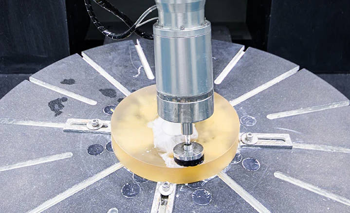
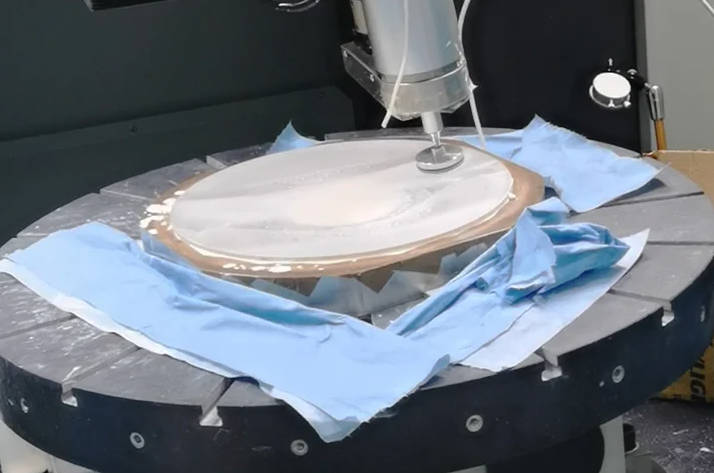
In modern manufacturing, metrology data is exported as a digital file and fed directly into computer-controlled polishing machines. This process, known as Computer Numerical Control (CNC) Polishing or Ion Beam Figuring (IBF), allows for “deterministic” polishing. Instead of an optician guessing where to polish, the machine uses the metrology map to apply extra pressure or dwell time on exactly the spots that are too high.
This “metrology-led correction” is the only way to achieve the extreme tolerances required for modern lithography and satellite optics.
VI. Frequently Asked Questions (FAQ)
1. Is λ/20 always better than λ/10?
In terms of precision, yes. However, in terms of value, not always. Increasing the precision from λ/10 to λ/20 can double or triple the cost of the part. If your system is limited by other factors (like atmospheric turbulence or sensor resolution), you may be paying for precision you cannot use.
2. Why does my metrology report look different from my colleague’s?
Measurements can be affected by “environmental noise.” Vibrations from a nearby truck, air currents in the room, or even a 1-degree change in temperature can alter an interferometer’s reading. High-quality optical polishing services perform measurements in vibration-isolated, temperature-controlled cleanrooms to ensure accuracy.
3. What is “Clear Aperture” (CA)?
Metrology is usually only guaranteed over the “Clear Aperture”—typically the central 90% of the optic. The edges of a lens are notoriously difficult to measure and polish perfectly, so it is important to define exactly where the light will actually pass through.
4. Can you measure aspheric surfaces?
Yes, but it is more complex. Aspheres (non-spherical shapes) require “null lenses” or computer-generated holograms (CGHs) to “cancel out” the complex shape so the interferometer can read it. This adds to the setup cost but is essential for modern compact lens designs.
VII. Conclusion: Choosing a Partner, Not Just a Vendor
Surface quality is the foundation of optical performance, but that quality is only as reliable as the metrology used to verify it. When you are looking for optical polishing services, don’t just ask about their polishing machines—ask about their metrology lab.
A sincere and professional partner will help you balance your technical needs with your budget, ensuring you don’t over-specify roughness where it isn’t needed, but also ensuring that critical “Surface Figure” errors are caught before the part ever leaves the shop.
By understanding the science of metrology, you move from being a “buyer” to being an informed engineer, capable of ensuring the success of your most ambitious optical projects.
Summary FAQ for Quick Review
- What is the “Figure” of an optic? It is the overall accuracy of the shape (e.g., how flat or spherical it is).
- What is “Roughness”? It is the micro-texture of the surface that causes light scatter.
- How is surface quality usually specified? Usually in fractions of a laser wavelength (λ), such as λ/10.
- What is the difference between P-V and RMS? P-V is the absolute difference between the highest and lowest points; RMS is the statistical average of the surface deviations.
- Which tool is used for most measurements? The Laser Interferometer is the primary tool for measuring surface figure.
- Why is metrology important for the customer? It provides mathematical proof that the component meets the required performance standards.