Key Takeaways
- Lithography optics require surface accuracies measured in fractions of a nanometer—far beyond conventional manufacturing capabilities
- EUV lithography demands super-polished surfaces with zero defects for 13.5nm wavelength operation
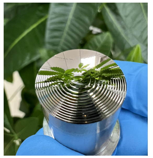
- Ultra-precision machining achieves Ra <1nm surface finishes enabling next-generation semiconductor production
- Fused silica and calcium fluoride remain primary materials for DUV lithography optics
- Nanometer-level tolerance control is essential for maintaining wavefront quality in projection systems
- YISHUN Optical’s precision manufacturing capabilities support semiconductor optical component development
Modern semiconductor manufacturing represents the pinnacle of precision engineering, with lithography systems producing features measured in single-digit nanometers. At the heart of these systems lie optical components whose precision requirements exceed what most engineers would believe possible. Understanding how these requirements are achieved—and the manufacturing challenges involved—illuminates the extraordinary capabilities of ultra-precision optical manufacturing.
The Critical Role of Lithography Optics
Semiconductor lithography transfers circuit patterns from photomasks onto silicon wafers through optical projection. This process repeats hundreds of times during chip fabrication, with each layer requiring precise pattern transfer. Optical system performance directly determines:
- Minimum feature sizes achievable
- Overlay accuracy between layers
- Defect density in finished devices
- Throughput and yield of the manufacturing process
As chipmakers push toward sub-3nm technology nodes, lithography optics requirements become increasingly demanding, requiring manufacturing capabilities that push the boundaries of human engineering.
Lithography System Architectures
Different lithography approaches impose varying requirements on optical components:
DUV (Deep Ultraviolet) Lithography
DUV systems using 193nm ArF excimer lasers remain the workhorse of semiconductor manufacturing. Projection optics must operate at this wavelength with exceptional wavefront quality:
- Numerical apertures exceeding 1.35
- Resolution enhancement through immersion technology
- Wavefront accuracy measured in millwaves
- Extremely low wavefront distortion over decades of operation
EUV (Extreme Ultraviolet) Lithography
EUV systems operating at 13.5nm represent the cutting edge of semiconductor manufacturing. These systems impose requirements that seemed impossible just decades ago:
- Grazing incidence reflective optics replace refractive designs
- Surface accuracy below 0.1nm RMS
- Surface roughness below 0.2nm RMS
- Defect densities approaching zero
- Multilayer reflective coatings with Angstrom-level precision
Surface Accuracy Requirements
Lithography optics surface accuracy specifications are measured in units that can be difficult to comprehend.
Traditional Optical Tolerances
Conventional optics specify surface accuracy in waves (λ) of light:
- λ/4 PV (peak-to-valley): Acceptable for many applications
- λ/10 PV: High-quality imaging optics
- λ/20 PV: The limit of traditional polishing
Lithography Optical Tolerances
Lithography optics exceed these traditional limits by orders of magnitude:
- Fractions of a wave at operating wavelengths
- 0.5nm RMS typical for advanced DUV systems
- 0.1nm RMS for EUV optics
- Angstrom-level surface figure control
To put this in perspective: one Angstrom equals 0.1nm, roughly the diameter of a hydrogen atom. Creating surfaces with this precision requires manufacturing processes of extraordinary sophistication.
Surface Roughness Requirements
Beyond overall figure accuracy, lithography optics require exceptional surface smoothness:
Sources of Surface Roughness Requirements
Surface roughness affects lithography performance through multiple mechanisms:
- Light scatter reducing system transmission
- Phase errors distorting the wavefront
- Defects causing pattern transfer errors
- Scatterometry measurement artifacts
Specification Levels
| System Type | Surface Roughness Requirement | Manufacturing Approach |
|---|---|---|
| Conventional optics | Ra <1nm | Standard polishing |
| Advanced DUV | Ra <0.5nm | Magnetorheological finishing |
| EUV optics | Ra <0.2nm | Ion beam figuring + super-polishing |
| Metrology reference | Ra <0.1nm | Specialized processes |
Super-Polishing Technology
Achieving sub-Angstrom surface roughness requires super-polishing technologies beyond traditional abrasive processes:
- Ion beam figuring removes material at atomic levels
- Magnetorheological finishing (MRF) provides computer-controlled material removal
- Elastic emission machining (EEM) employs chemical-mechanical effects
- Plasma polishing uses activated gas species for surface modification
Material Requirements for Lithography Optics
Material selection for lithography optics balances multiple factors including transmission, thermal stability, homogeneity, and machinability.
Fused Silica (SiO2)
Fused silica remains the dominant material for DUV lithography optics:
- Excellent transmission at 193nm wavelength
- Extremely low thermal expansion coefficient
- High homogeneity achievable through careful processing
- Challenging to machine due to hardness and brittleness
Calcium Fluoride (CaF2)
Calcium fluoride crystals serve as lens elements in advanced DUV systems:
- Superior transmission characteristics at 193nm
- Good homogeneity and thermal stability
- Single-crystal structure enables precise machining
- Requires careful handling due to cleavage susceptibility
EUV Optics Materials
EUV systems employ reflective optics requiring entirely different material approaches:
- Ultra-low expansion glass (ULE) for substrate stability
- Multilayer coatings of silicon and molybdenum
- Zero-defect surfaces because EUV cannot tolerate particles
Manufacturing Challenges in Lithography Optics
Producing lithography-quality optics involves challenges rarely encountered in other precision manufacturing contexts.
Subsurface Damage Control
Traditional grinding and polishing processes introduce subsurface damage that compromises surface integrity:
- Damage depths of microns from conventional grinding
- Even gentle polishing can leave subsurface cracks
- Ion beam and plasma processes minimize subsurface damage
- Specialized measurement techniques required for detection
Environmental Control
Lithography optics manufacturing requires exceptional environmental control:
- Temperature stability within fractions of a degree
- Humidity control preventing moisture adsorption
- Vibration isolation during measurement and processing
- Cleanroom conditions eliminating particulate contamination
Metrology Limitations
Measuring what you need to make requires measurement capabilities matching the precision required:
- Interferometric testing with Angstrom-level resolution
- Phase-shifting interferometry for surface figure
- Atomic force microscopy for roughness measurement
- X-ray diffraction for crystal structure verification
Manufacturing Process Sequences
Producing lithography-quality optics follows sophisticated multi-step processes:
Lens Manufacturing Sequence
- Material verification: Incoming inspection confirming optical homogeneity
- Rough shaping: Diamond turning or grinding to near-net shape
- Fine grinding: Progressive abrasive steps reducing subsurface damage
- Computer-controlled polishing: MRF or CNC polishing achieving figure accuracy
- Super-polishing: Final material removal for sub-nanometer roughness
- Cleaning: Multi-step cleaning removing all contamination
- Coating: Anti-reflective or reflective coatings as required
- Final inspection: Complete verification before shipping
Mirror Manufacturing Sequence
- Substrate fabrication: Machining or grinding to final form
- Surface preparation: Achieving baseline surface quality
- Figure correction: Computer-controlled figuring to final accuracy
- Super-finishing: Achieving required surface smoothness
- Cleaning and verification: Particle-free surface confirmation
- Reflective coating: Multilayer coating deposition
- Final metrology: Complete optical testing
Quality Verification for Lithography Optics
Verification of lithography optics requires the most sophisticated metrology available:
Interferometric Surface Testing
Zygo interferometers and similar systems provide surface figure measurement:
- Sub-nanometer resolution over large apertures
- Multiple wavelength testing for surface form verification
- Computer-generated holograms for aspheric testing
- Environmental isolation during measurement
Wavefront Testing
Full system testing verifies optical performance:
- Hartmann-Shack wavefront sensors
- Through-focus testing
- Star image analysis
- Modulation transfer function (MTF) measurement
Defect Detection
Advanced inspection systems identify surface defects:
- Light scattering measurement (TIS testing)
- Automated defect detection and classification
- Coded aperture inspection for EUV optics
- DUV inspection for critical surfaces
Tolerance Analysis and Error Budgets
Lithography optical systems allocate error budgets across multiple contributors:
Wavefront Error Budget
System wavefront error typically allocates:
- Surface figure contribution from each element
- Assembly and alignment tolerances
- Coating phase errors
- Environmental effects
- Temporal stability requirements
Stray Light and Scatter Budget
Total integrated scatter (TIS) must remain below acceptable limits:
- Surface roughness contribution
- Micro-roughness effects
- Bulk scatter from material inhomogeneity
- Edge effects and coating non-uniformity
Emerging Requirements for Next-Generation Lithography
As semiconductor technology advances, lithography optics requirements continue tightening:
High-NA EUV
Next-generation EUV systems will employ numerical apertures approaching 0.55:
- Even stricter surface accuracy requirements
- Novel mirror designs with complex geometries
- New coating technologies with improved reflectivity
- Enhanced defect sensitivity
3nm and Beyond
Advanced nodes require:
- Improved overlay accuracy
- Enhanced resolution enhancement techniques
- Tighter CD uniformity control
- Reduced pattern fidelity sensitivity
Supply Chain Considerations for Lithography Optics
The lithography optics supply chain involves specialized manufacturers:
Equipment Manufacturers
Companies like ZEISS and Nikon manufacture complete lithography optical systems:
- Vertical integration of component manufacturing
- Proprietary processes developed over decades
- Extreme capital investment in capabilities
- Limited number of qualified suppliers globally
Component Suppliers
Supporting manufacturers provide:
- Substrate materials (Corning, Ohara)
- Coating services (Ion Beam Services, Optics Balzers)
- Precision machining (YISHUN Optical and similar specialists)
- Metrology services and calibration
Qualification Requirements
Component suppliers must demonstrate:
- Extreme precision manufacturing capability
- Advanced metrology and verification
- Quality system compliance
- Long-term stability and supply assurance
Supporting Technologies and Precision Machining
While lithography optics themselves require specialized manufacturing, supporting optical components for lithography equipment benefit from ultra-precision machining:
- Vacuum chamber components requiring sub-micron tolerances
- Motion control elements with exceptional straightness
- Reference surfaces for calibration and alignment
- Structural elements with thermal stability
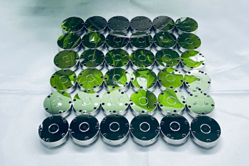
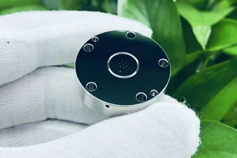
YISHUN Optical’s capabilities in precision machining complement lithography optics manufacturing by producing these supporting components with consistent quality and precision.
Conclusion
Semiconductor lithography optics represent the extreme end of precision manufacturing, requiring capabilities measured in Angstroms and surface qualities that seemed impossible just decades ago. Meeting these requirements demands extraordinary investment in manufacturing equipment, process development, environmental control, and metrology capabilities.
While YISHUN Optical’s capabilities may not directly produce production lithography optics—those require investments exceeding what any commercial supplier could justify—the principles and techniques of ultra-precision manufacturing apply throughout the semiconductor equipment supply chain. Supporting components, reference optics, and precision machined elements all benefit from the same commitment to precision that defines lithography optics manufacturing.
Understanding these extreme requirements illuminates what’s possible in precision manufacturing and informs discussions of optical component capabilities across demanding applications.
Frequently Asked Questions
What surface accuracy is required for semiconductor lithography optics?
Advanced DUV lithography optics require surface accuracies of approximately 0.5nm RMS, while EUV optics demand even tighter specifications below 0.1nm RMS. These requirements exceed what conventional manufacturing can achieve.
Why is surface roughness so critical for lithography optics?
Surface roughness causes light scattering that reduces system transmission and introduces phase errors affecting pattern fidelity. At advanced technology nodes, even sub-nanometer roughness affects device performance.
What materials are used for lithography optics?
Fused silica dominates DUV lithography applications, with calcium fluoride used for specific elements. EUV optics employ ultra-low expansion glass substrates with silicon-molybdenum multilayer coatings.
How are lithography optics manufactured?
Manufacturing involves multi-step processes including grinding, computer-controlled polishing, magnetorheological finishing, ion beam figuring, and super-polishing. Complete manufacturing sequences can span months for single optics.
Why is subsurface damage a concern for lithography optics?
Subsurface damage creates local stress concentrations and phase errors that affect optical performance. Super-polishing processes minimize subsurface damage but cannot eliminate it entirely.
What metrology is required for lithography optics verification?
Verification requires interferometric surface testing, wavefront measurement, atomic force microscopy for roughness, and advanced defect detection systems. Metrology capabilities must match or exceed manufacturing tolerances.
How does EUV lithography differ from DUV in optical requirements?
EUV uses reflective optics operating at 13.5nm wavelength rather than refractive optics at 193nm. This requires different materials (multilayer coatings), grazing incidence geometries, and even stricter surface requirements.
Interested in precision optical components for semiconductor equipment applications? Contact YISHUN Optical at info@yishunoptical.com or visit yishunoptical.com to discuss your precision manufacturing requirements.