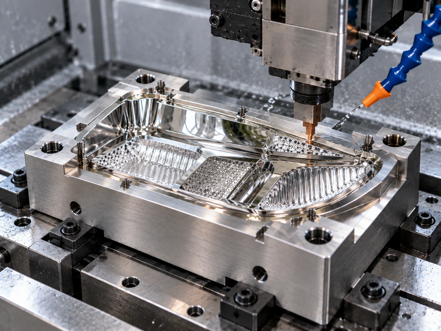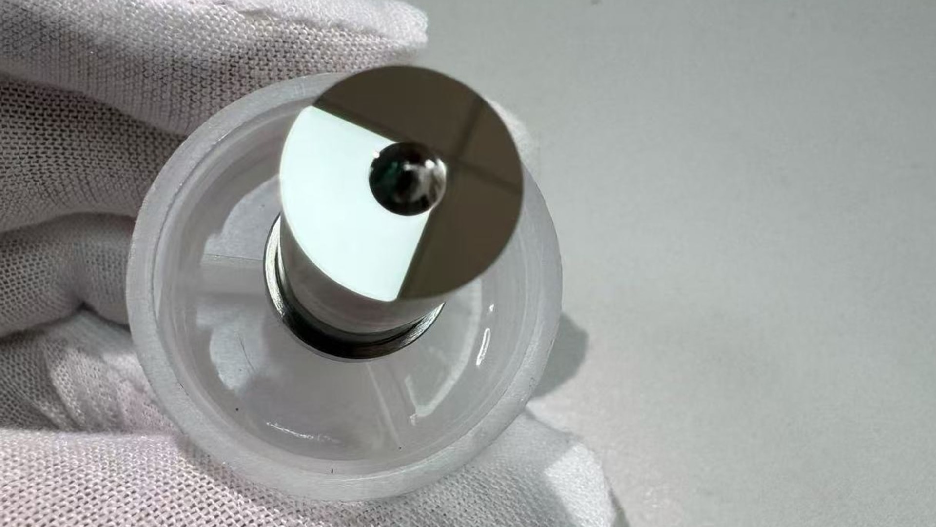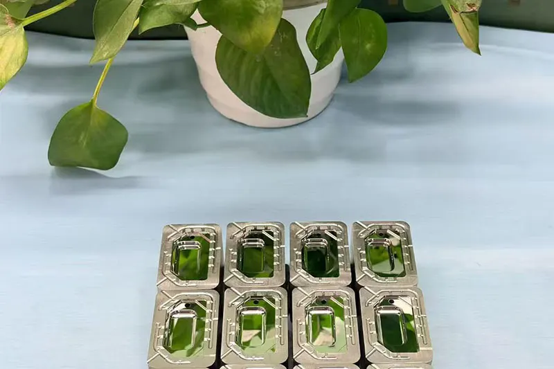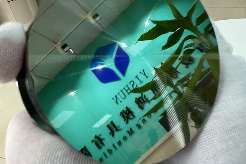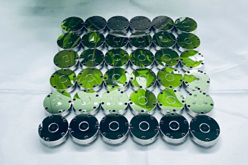
Optical polishing defects are surface or geometry problems that appear during or after precision polishing, such as scratches, edge chips, pits, haze, polishing marks, orange peel, warping, and poor flatness. These defects can affect light transmission, reflection, coating quality, assembly accuracy, and long-term component reliability.
In optical manufacturing, polishing is not only a cosmetic process. It is a controlled finishing step used to produce functional surfaces for optical windows, lenses, mirrors, prisms, wafers, substrates, laser components, and precision technical parts. When polishing defects are not controlled, a component may fail inspection even if its size and material are correct.
For B2B buyers, understanding common optical polishing defects helps improve drawing specifications, supplier communication, quality inspection, and RFQ accuracy. It also helps determine whether a project needs lapping, polishing, re-polishing, edge protection, or a different process route.
YISHUN Optical provides optical polishing and lapping services for custom optical components that require controlled surface quality, flatness, roughness, and defect prevention.
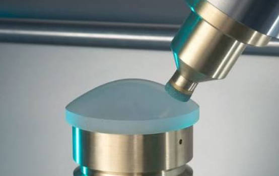
Why Optical Polishing Defects Matter
Optical components interact directly with light. A defect that looks small under normal lighting may still create functional problems in laser, imaging, photonics, semiconductor, and metrology applications.
Optical polishing defects may cause:
- Increased light scattering
- Reduced transmission
- Unstable reflection
- Coating adhesion problems
- Beam distortion
- Image quality loss
- Assembly misalignment
- Bonding or sealing issues
- Lower production yield
- Inspection rejection
- Reduced component reliability
For optical components, surface quality is often as important as dimensional accuracy because light passes through or reflects from the polished surface.
For example, a polished optical window with scratches may scatter light. A mirror substrate with polishing marks may affect reflection quality. A sapphire component with edge chips may fail during mounting. A thin substrate with warping may cause bonding or flatness issues.
This is why optical polishing defects should be addressed through process control, material understanding, proper pre-processing, clear specifications, and reliable inspection.
Common Optical Polishing Defects at a Glance
| Defect Type | Typical Appearance | Possible Impact |
|---|---|---|
| Scratches | Long or short lines on the surface | Scattering, visual rejection, coating issues |
| Edge chips | Small broken areas along edges | Handling risk, assembly failure, crack growth |
| Pits or digs | Small holes or local depressions | Surface quality failure, scattering |
| Haze | Cloudy or foggy surface appearance | Reduced clarity and transmission |
| Polishing marks | Directional or irregular marks | Poor surface quality, optical inconsistency |
| Orange peel | Uneven texture similar to orange skin | Surface roughness and cosmetic/functional defects |
| Warping | Part bends or deviates from intended geometry | Poor flatness, assembly or bonding problems |
| Poor flatness | Surface does not meet geometry requirement | Optical path error, poor contact |
| Embedded particles | Contaminants trapped on or in surface | Scratches, coating failure, contamination risk |
| Subsurface damage | Hidden damage from earlier grinding or cutting | Later cracking, low polishing yield |
Most optical polishing defects are caused by a combination of material behavior, pre-processing quality, abrasive control, cleaning, pressure, fixture design, and handling.
1. Optical Polishing Scratches
Scratches are one of the most common defects in optical polishing. They may appear as fine lines, random marks, deep cuts, or directional scratches. Some scratches are visible under standard inspection, while others require magnification or controlled lighting.
Common Causes of Scratches
Optical polishing scratches may be caused by:
- Abrasive contamination
- Large particles in slurry
- Dirty polishing pads
- Poor cleaning between process steps
- Hard particles trapped on the surface
- Improper handling
- Contact with tools, trays, or fixtures
- Reusing contaminated packaging
- Incomplete removal of grinding damage
How Scratches Affect Optical Components
Scratches can reduce optical clarity, increase scattering, affect coating quality, and cause inspection failure. In laser applications, surface scratches may become local stress or absorption points depending on the material and use environment.
How to Avoid Scratches
To reduce optical polishing scratches, suppliers should control abrasive cleanliness, pad condition, cleaning steps, handling methods, and inspection procedures.
Practical prevention methods include:
| Prevention Method | Purpose |
|---|---|
| Use clean slurry and controlled abrasive size | Reduces risk of large-particle scratches |
| Clean parts between processing stages | Prevents coarse abrasive transfer |
| Maintain polishing pads properly | Avoids embedded particles and uneven contact |
| Use suitable fixtures and carriers | Reduces accidental surface contact |
| Handle parts with clean tools and gloves | Prevents fingerprints and hard particle damage |
| Inspect before and after polishing | Identifies whether scratches come from previous steps |
To avoid scratches in optical polishing, contamination control is just as important as polishing technique.
2. Edge Chips and Edge Cracks
Edge chips are small broken areas along the edge of an optical component. They are common in brittle materials such as glass, quartz, fused silica, sapphire, ceramics, and some optical crystals.
Common Causes of Edge Chips
Edge chips may occur during cutting, grinding, lapping, polishing, cleaning, inspection, packaging, or assembly. Common causes include:
- Brittle material behavior
- Sharp unprotected edges
- Excessive processing pressure
- Poor edge bevel or chamfer design
- Improper fixturing
- Impact during handling
- Contact between parts
- Aggressive cleaning or drying
- Incorrect packaging
Why Edge Chips Are a Problem
Edge chips can affect assembly, sealing, mechanical strength, and visual quality. In some cases, small edge chips may grow into larger cracks under stress, vibration, or thermal cycling.
How to Avoid Edge Chips
Edge protection should be considered before polishing begins. A small bevel, chamfer, or edge specification may help reduce chipping risk, depending on the component design.
| Prevention Method | Benefit |
|---|---|
| Specify edge chamfer or bevel | Reduces sharp-edge breakage |
| Use proper fixtures | Supports the part during processing |
| Control polishing pressure | Reduces stress on fragile edges |
| Separate parts during cleaning and packaging | Prevents part-to-part impact |
| Use suitable trays and protective packaging | Reduces transport damage |
| Discuss edge quality in RFQ | Prevents misunderstanding during inspection |
For fragile optical parts, edge requirements should be included in drawings or purchasing specifications, not left as an afterthought.
3. Pits, Digs and Small Surface Depressions
Pits and digs are small depressions, holes, or localized surface defects. They may come from material inclusions, grinding damage, abrasive issues, or incomplete polishing.
Common Causes
Pits and digs may be caused by:
- Material defects
- Pull-out of inclusions
- Deep grinding marks
- Subsurface damage
- Coarse abrasive damage
- Incomplete polishing time
- Chemical reaction with slurry or cleaning agents
- Surface contamination
How They Affect Performance
Pits and digs can scatter light, affect coating uniformity, reduce cosmetic quality, and cause inspection failure. In high-precision optical parts, even small surface defects may be unacceptable depending on the application.
Prevention Methods
The key to reducing pits and digs is to control earlier process steps. Polishing alone may not remove deep defects efficiently.
Recommended actions include:
- Use proper grinding and lapping before polishing
- Avoid overly aggressive material removal
- Select suitable abrasive and slurry chemistry
- Inspect the surface before final polishing
- Confirm whether defects are material-related or process-related
- Allow enough removal depth if previous damage exists
If a component already has deep pits, re-polishing may not be enough. Additional lapping or grinding may be required before final polishing.
4. Haze and Cloudy Surface Appearance
Haze is a cloudy, foggy, or milky surface condition that reduces clarity. It may be uniform across the surface or appear in specific areas.
Common Causes of Haze
Haze may result from:
- Incomplete polishing
- Incorrect slurry or pad selection
- Chemical residue
- Fine scratches
- Poor cleaning
- Surface contamination
- Material reaction
- Inconsistent polishing pressure
- Inadequate final finishing step
Why Haze Matters
Haze can reduce transmission, increase scattering, and make optical components unsuitable for imaging, laser, or inspection applications. It may also indicate that the surface roughness or cleaning process is not properly controlled.
How to Avoid Haze
Haze prevention depends on matching the polishing method to the material and final application.
| Cause | Prevention |
|---|---|
| Incomplete polishing | Use suitable polishing time and fine finishing process |
| Residue | Improve cleaning and drying process |
| Pad mismatch | Select pad based on material and surface target |
| Fine scratches | Improve contamination control |
| Material reaction | Review slurry chemistry and cleaning method |
For quartz, fused silica, sapphire, and specialty optical materials, haze control may require material-specific polishing experience.
5. Polishing Marks and Tool Patterns
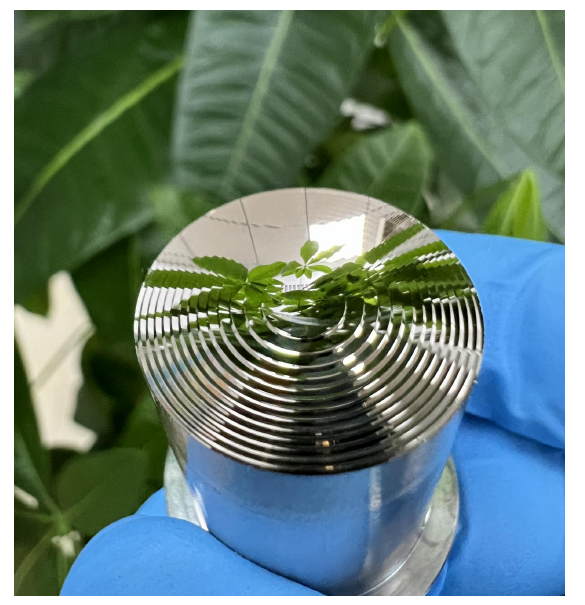
Polishing marks are visible or measurable patterns left by the polishing process. They may appear as directional marks, swirl marks, uneven zones, circular patterns, or non-uniform surface texture.
Common Causes
Polishing marks can come from:
- Uneven pressure
- Poor pad condition
- Incorrect motion path
- Unstable fixture
- Inconsistent slurry distribution
- Excessive processing force
- Part movement during polishing
- Improper transition from rough to fine polishing
Impact on Optical Performance
Polishing marks may reduce surface quality, create optical inconsistency, and affect coating or reflection. For mirrors, windows, and precision substrates, polishing marks may be unacceptable even if the part appears generally clear.
Prevention Methods
To reduce polishing marks, the process must be stable and repeatable. Important controls include pressure, pad conditioning, abrasive selection, fixture design, and cleaning between steps.
YISHUN Optical supports precision optical polishing and lapping services for components that require controlled surface finishing and geometry preparation.
6. Orange Peel Defect in Optical Polishing
Orange peel describes a textured surface that looks uneven, similar to the skin of an orange. It is usually related to surface roughness, material response, pad behavior, or process instability.
Common Causes
Orange peel may be caused by:
- Improper polishing pressure
- Incorrect pad hardness
- Material microstructure response
- Inconsistent abrasive action
- Inadequate fine polishing
- Previous process damage
- Poor control of slurry condition
Why It Matters
Orange peel can affect optical appearance, surface roughness, reflection quality, and coating readiness. It may be more noticeable on reflective surfaces or components with strict cosmetic requirements.
How to Avoid Orange Peel
Preventing orange peel usually requires adjusting the polishing process, including pad selection, slurry, pressure, polishing time, and pre-polishing surface condition.
For sensitive optical parts, trial polishing may be useful during prototype development before production quantities are processed.
7. Warping and Poor Flatness
Warping occurs when a component bends, distorts, or loses its intended geometry during processing. Poor flatness means the polished surface does not meet the required plane accuracy.
Common Causes
Warping and poor flatness may be caused by:
- Thin part geometry
- Internal material stress
- Uneven material removal
- Excessive pressure
- Poor support during polishing
- Thermal effects
- Inadequate lapping before polishing
- Incorrect fixture design
- Stress release after cutting or grinding
Why It Matters
Flatness is important for optical windows, substrates, wafers, mirrors, bonding surfaces, and sealing components. Poor flatness can cause beam deviation, assembly gaps, coating issues, bonding failure, or unstable mechanical contact.
Lapping is often required before polishing when flatness, parallelism, or thickness uniformity must be controlled.
How to Avoid Warping
Warping prevention starts before polishing. The supplier must evaluate material, thickness, geometry, support method, and process pressure.
Practical methods include:
- Use lapping before final polishing when flatness is critical
- Control material removal evenly
- Avoid excessive pressure on thin parts
- Use proper fixtures and carriers
- Consider stress relief or process sequencing when needed
- Inspect flatness between process stages
- Discuss realistic flatness requirements before production
For custom optical components, combined lapping and polishing can help control both geometry and surface quality.
Defect Prevention by Process Stage
Optical polishing defect control should be built into the full process, not only the final polishing step.
| Process Stage | Main Risk | Prevention Focus |
|---|---|---|
| Material selection | Inclusions, stress, poor polishability | Choose suitable material grade and review application |
| Cutting and grinding | Subsurface damage, chips | Control cutting method and grinding parameters |
| Lapping | Poor flatness, embedded particles | Use suitable abrasive and clean process control |
| Rough polishing | Scratches, uneven removal | Control pressure, pad, slurry, and cleaning |
| Fine polishing | Haze, polishing marks, roughness | Use stable finishing process and clean environment |
| Cleaning | Residue, contamination, scratches | Use proper cleaning method and handling |
| Inspection | Missed defects, unclear acceptance | Define inspection method and criteria |
| Packaging | Scratches, edge chips, contamination | Use protective and clean packaging |
This table shows why supplier process discipline is critical. Many visible defects in final polishing actually begin in earlier stages.
How Buyers Can Reduce Optical Polishing Defects
Buyers can reduce polishing defects by providing clear requirements and communicating application needs early.
Provide Complete Drawings
A useful drawing should define dimensions, material, surface requirements, edge quality, flatness, parallelism, and any critical functional areas.
Specify Surface Quality Clearly
Avoid vague phrases such as “good polish” or “optical finish” without measurable requirements. Use roughness, scratch-dig, flatness, or application-based standards when appropriate.
Share the Final Application
The supplier should know whether the part will be used for transmission, reflection, coating, bonding, sealing, laser exposure, imaging, or mechanical contact.
Confirm Lapping Requirements
If flatness or parallelism matters, confirm whether lapping is needed before polishing. Polishing alone may not correct geometry problems efficiently.
Discuss Inspection Criteria
Inspection methods should be agreed before production. This reduces disputes and helps the supplier plan the process correctly.
Consider Prototype Testing
For new materials, thin parts, difficult geometries, or strict surface requirements, prototype polishing can help identify risks before production.
How to Choose an Optical Polishing Supplier
A reliable optical polishing supplier should have process experience, material knowledge, inspection capability, and clear communication. Price alone is not enough when surface quality and yield are critical.
When evaluating a supplier, check the following:
| Supplier Capability | Why It Matters |
|---|---|
| Material experience | Different materials polish differently |
| Lapping and polishing capability | Helps control geometry and surface quality together |
| Defect prevention process | Reduces scratches, edge chips, haze, and marks |
| Inspection support | Confirms whether parts meet agreed criteria |
| Engineering review | Helps identify risks before production |
| Cleaning and packaging control | Protects polished surfaces after processing |
| Prototype and production support | Helps move from samples to repeatable batches |
You can review YISHUN Optical’s optical polishing and lapping capabilities to evaluate whether the service direction matches your component requirements.
For company-level information and broader optical processing support, you can also visit YISHUN Optical.
RFQ Checklist for Avoiding Optical Polishing Defects
To help reduce polishing defects, include the following information in your RFQ:
| RFQ Item | Why It Helps |
|---|---|
| Material | Helps supplier select process and estimate risk |
| Drawing or CAD file | Defines geometry and critical features |
| Quantity | Supports prototype or production planning |
| Surface roughness | Defines surface finish target |
| Scratch-dig requirement | Defines acceptable surface defects |
| Flatness | Helps determine whether lapping is needed |
| Parallelism | Important for windows, plates, and substrates |
| Edge requirement | Helps prevent chips and cracks |
| Coating requirement | Defines cleanliness and surface preparation needs |
| Application | Helps prioritize functional areas |
| Inspection requirement | Defines acceptance method |
| Packaging requirement | Protects polished parts during shipment |
A complete RFQ helps the supplier identify polishing risks before production instead of discovering defects after the parts are finished.
Conclusion
Optical polishing defects such as scratches, edge chips, pits, haze, polishing marks, orange peel, warping, and poor flatness can affect optical performance, coating quality, assembly reliability, and production yield. Most defects are preventable when the process is planned correctly from material selection and pre-processing to polishing, cleaning, inspection, and packaging.
For buyers, the most effective way to reduce defects is to provide clear drawings, realistic specifications, application details, inspection criteria, and edge requirements. For suppliers, defect prevention depends on material experience, clean processing, stable lapping and polishing methods, careful handling, and reliable inspection.
If your project requires defect-controlled polishing for optical windows, lenses, mirrors, substrates, quartz, sapphire, glass, or custom optical components, YISHUN Optical can support your project with precision optical polishing and lapping services from requirement review to finished component delivery.
FAQ
What are the most common optical polishing defects?
The most common optical polishing defects include scratches, edge chips, pits, digs, haze, polishing marks, orange peel, warping, poor flatness, and embedded contamination. These defects may affect optical clarity, coating quality, reflection, transmission, and assembly reliability.
How do you avoid scratches in optical polishing?
Scratches can be reduced by controlling abrasive cleanliness, using clean polishing pads, cleaning parts between process stages, improving handling methods, and preventing particle contamination. Deep scratches from earlier grinding may require additional lapping or reprocessing.
What causes edge chips during optical polishing?
Edge chips are often caused by brittle materials, sharp unprotected edges, excessive pressure, poor fixturing, part-to-part contact, or improper handling. Adding suitable edge chamfers and using protective packaging can help reduce chipping risk.
Why does haze appear after optical polishing?
Haze may appear because of incomplete polishing, fine scratches, poor cleaning, chemical residue, material reaction, or incorrect pad and slurry selection. The prevention method depends on material type and required surface quality.
Can optical polishing remove pits and digs?
Polishing may remove shallow pits and digs, but deep defects may require additional grinding or lapping. Some pits may come from material inclusions or subsurface damage, so the supplier should inspect the component before confirming repair feasibility.
Why is flatness still poor after polishing?
Poor flatness after polishing may occur when the part was not properly lapped before polishing, when material stress caused warping, or when pressure and fixturing were not controlled. Lapping is often needed before polishing when flatness is critical.
What should I include in an RFQ to avoid optical polishing defects?
A useful RFQ should include material, drawing, dimensions, quantity, surface roughness, scratch-dig, flatness, parallelism, edge quality, coating requirements, application, inspection criteria, and packaging needs.