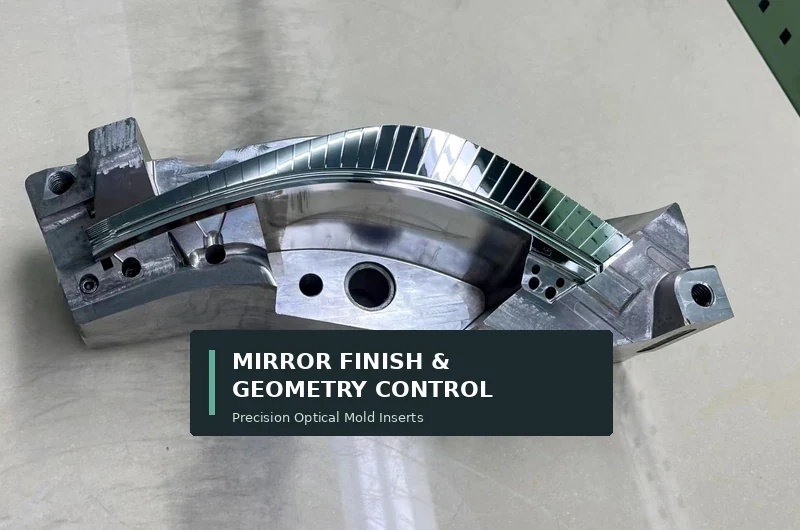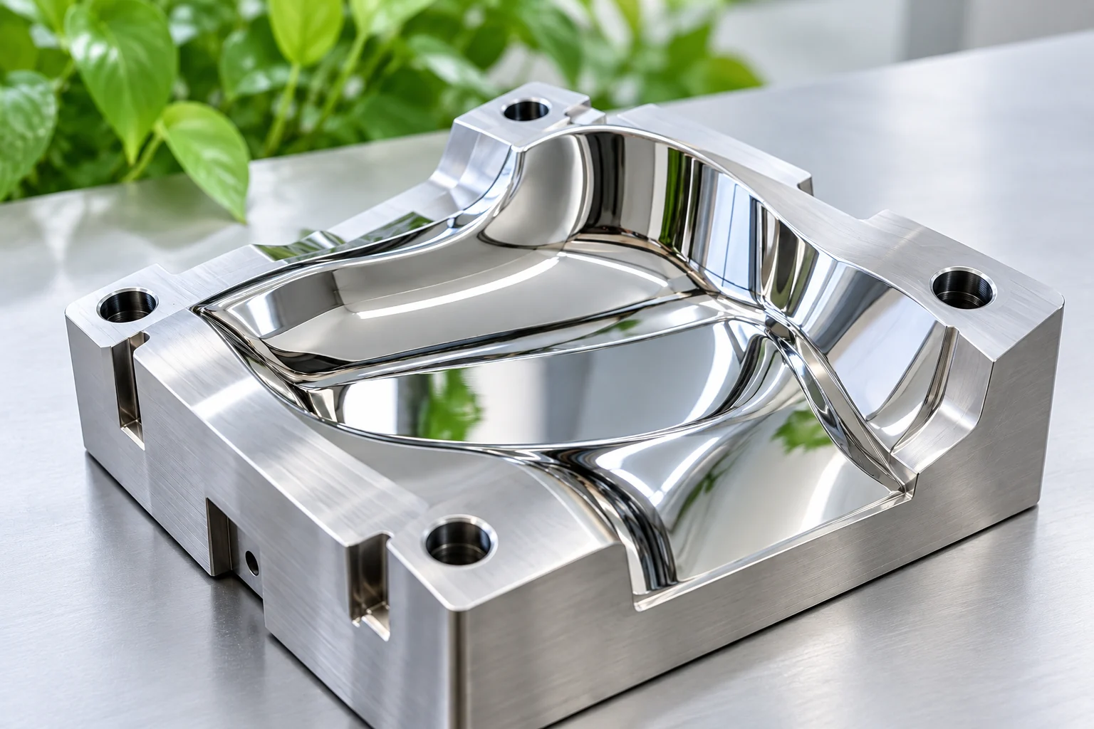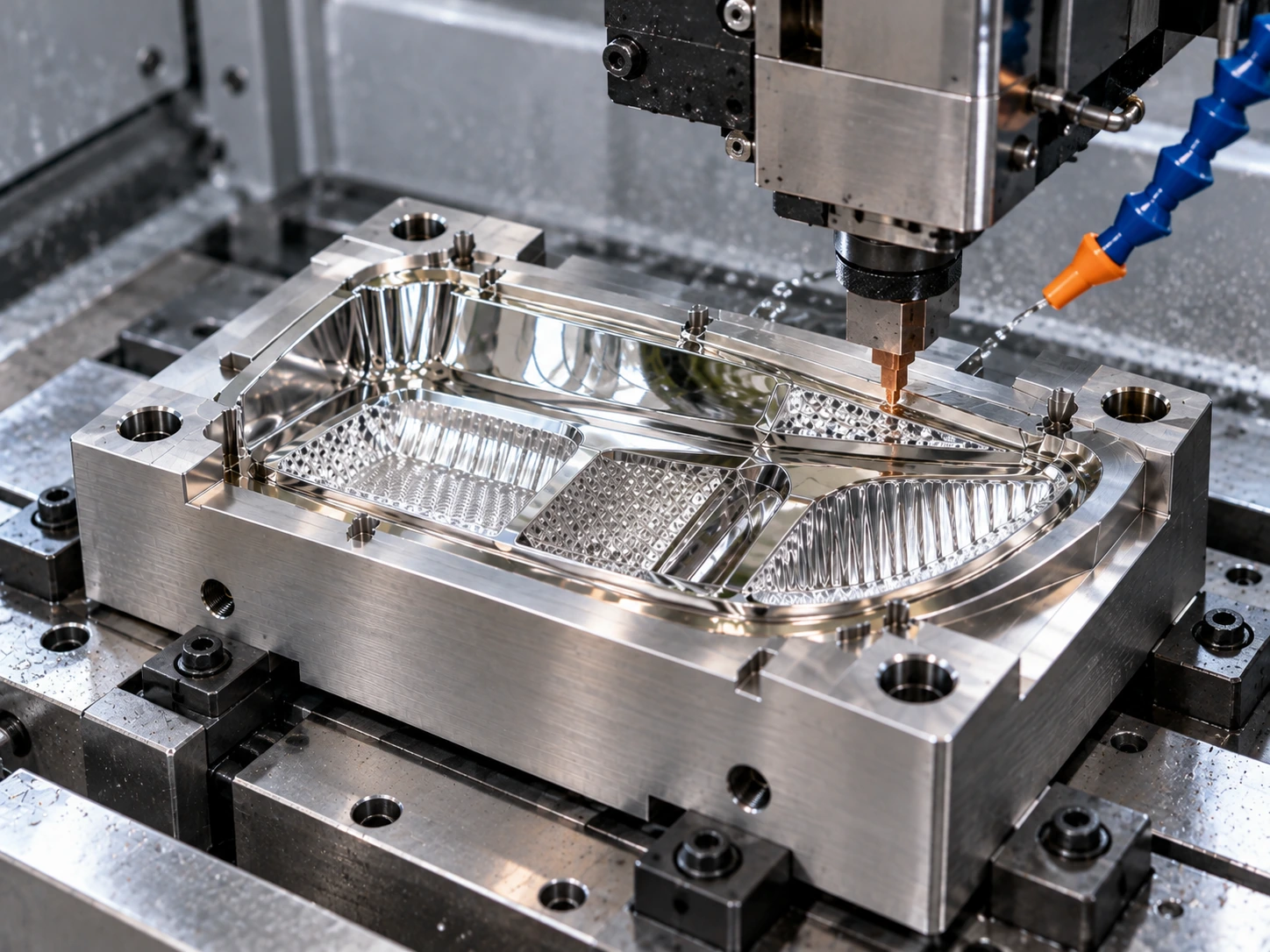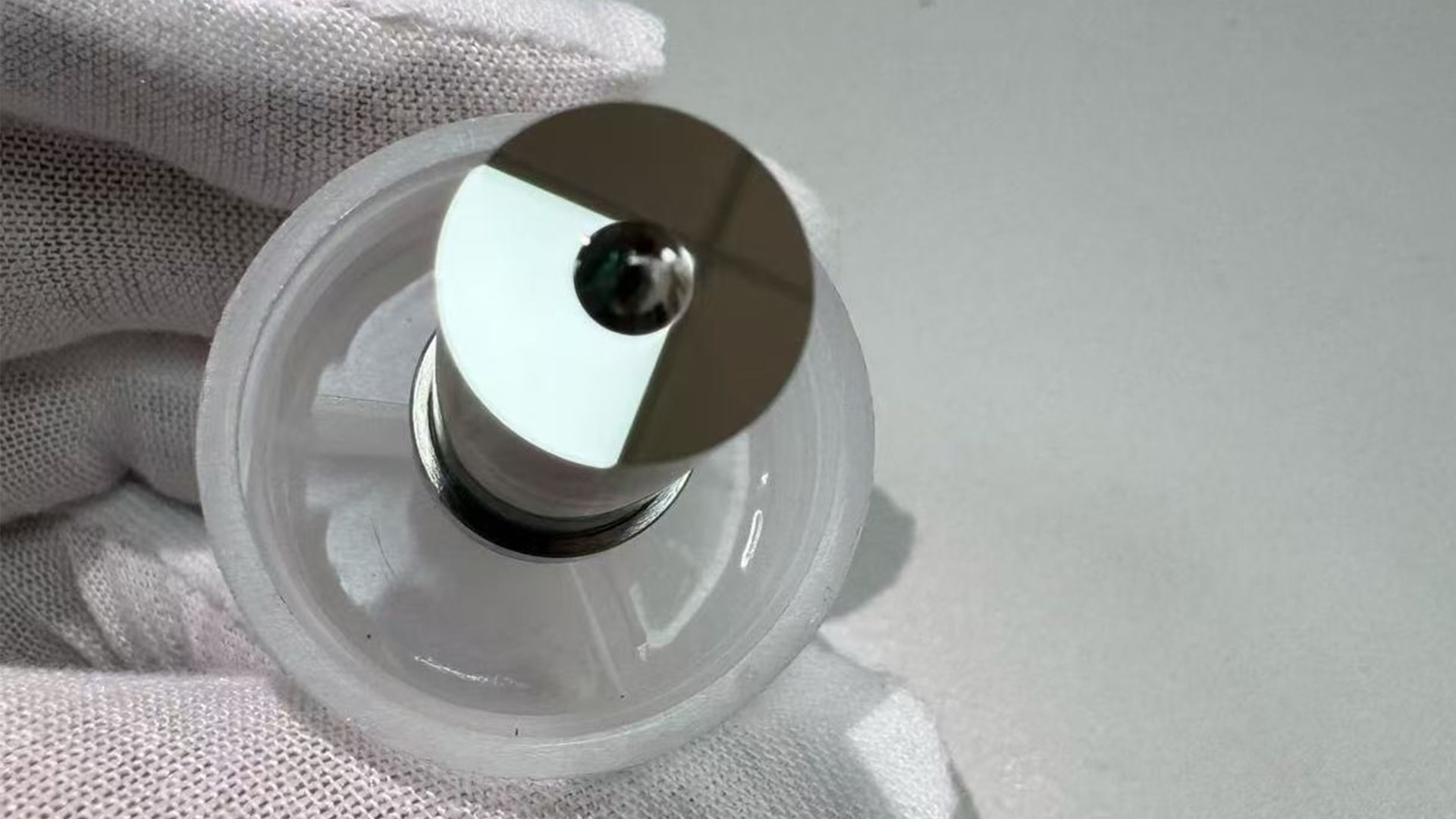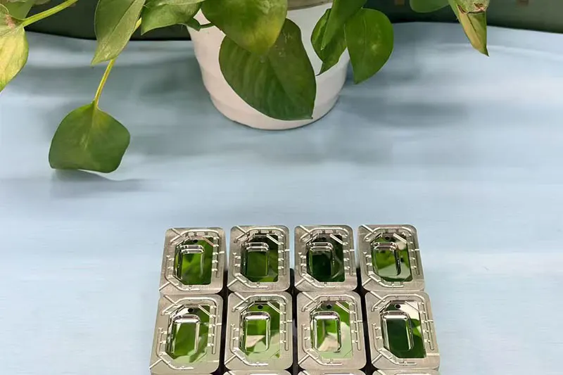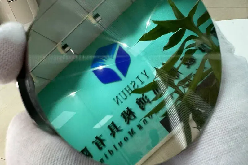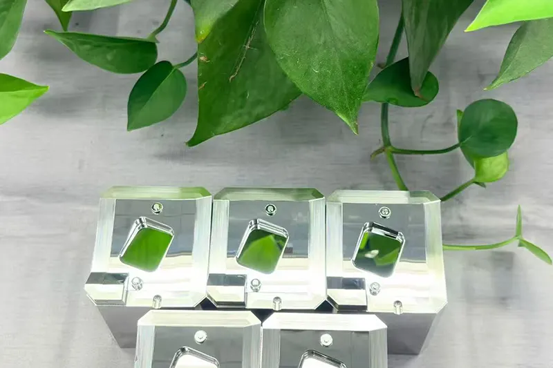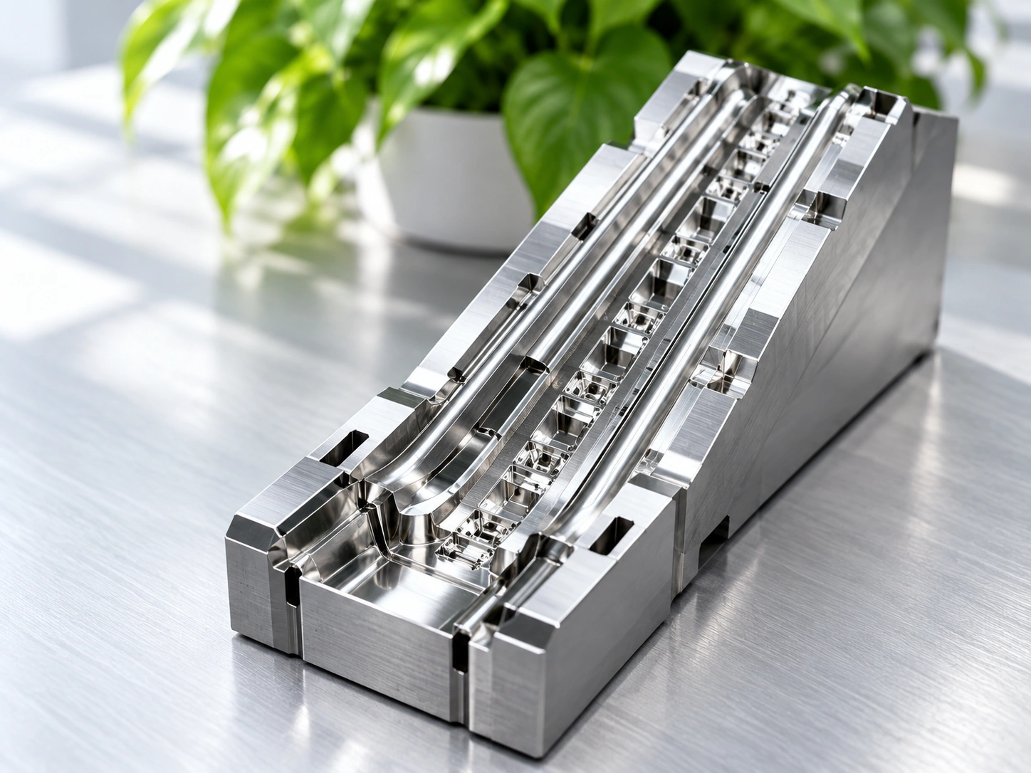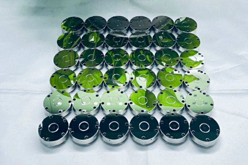
In precision injection tooling, mold surface condition directly dictates part optical clarity, light transmission efficiency, and surface fidelity. Achieving true optical-grade performance requires far more than aesthetic, mirror-like polishing; it demands sub-micron form accuracy, controlled surface roughness ($Ra$ values often well below 0.05 µm), and pristine edge retention. Selecting qualified optical polishing services comes down to matching substrate metallurgy with staged abrasive processes, maintaining geometry without edge roll-off, and verifying results with interferometric metrology.
This technical guide outlines the structural standards, metallurgy considerations, procedural transitions between lapping and polishing, and supplier evaluation criteria necessary to specify and source precision optical tooling without unexpected scrap or iterative mold trials.
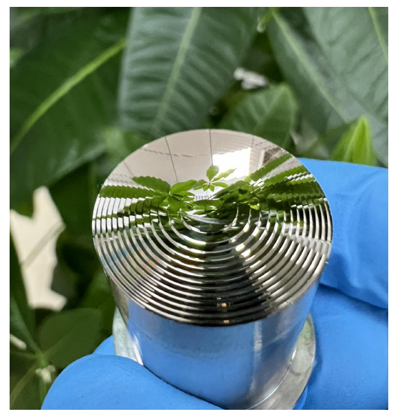
The Engineering Stakes of Optical Mold Finishing
A standard decorative mirror polish reflects light visibly, but it rarely functions as an optical surface. Under microscopic evaluation, conventional hand-polished tooling displays surface waviness, residual tool marks, and micro-grooves. In optical applications—such as camera lenses, automotive light guides, HUD mirrors, and medical diagnostic windows—these micro-irregularities refract, scatter, and distort light paths within the molded polymer.
The functional differences between standard and optical-grade mold finishes involve three critical physical properties:
- Wavefront and Form Error: Standard polishing tends to round edges and distort localized flatness. Optical tooling requires strict profile adherence to ensure nominal focal lengths and uniform beam dispersion across the molded optics.
- Scatter Losses (Haze): Incomplete scratch removal and uneven micro-roughness generate scattered light, reducing optical clarity and transmission efficiency.
- Parting Line Integrity: Over-polishing mold cavity edges causes parting-line roll-off, which immediately creates parting-line flash during high-pressure injection molding.
Specifying dedicated precision optical polishing services ensures the finishing process removes microscopic material uniformly while preserving the cavity’s coordinate datums and designated CAD geometry.
Standards and Metrics: Decoding Surface Roughness and SPI Classifications
Specifying an optical finish requires standard engineering units rather than subjective descriptions like “high-gloss” or “mirror.” The Society of the Plastics Industry (SPI) mold finish standards provide the baseline for North American tooling, while ISO and ASME standards use roughness average ($Ra$), root-mean-square roughness ($Rq$), and mean peak-to-valley height ($Rz$).
Optical mold inserts typically fall within SPI Class A, achieved through graded diamond compounds:
| SPI Class | Finishing Method / Abrasive | Typical Surface Roughness (Ra) | Typical Tooling Application |
| SPI A-1 | Grade 3 Diamond Buff (Fine) | $\approx$ 0.012 to 0.025 µm (0.5 to 1 µin) | High-precision camera lenses, medical optics, laser optics |
| SPI A-2 | Grade 6 Diamond Compound | $\approx$ 0.025 to 0.05 µm (1 to 2 µin) | Automotive light guides, transparent housings, display panels |
| SPI A-3 | Grade 15 Diamond Compound | $\approx$ 0.05 to 0.10 µm (2 to 4 µin) | General transparent parts, non-critical sight glasses, lighting bezels |
Note: Exact attainable $Ra$ values depend on base steel hardness, grain structure, and finishing technique.
For precision imaging and laser optics, SPI A-1 is often the entry threshold. Beyond SPI classifications, specialized optical tools may require sub-nanometer root-mean-square roughness ($Rq < 1\text{ nm}$) and specified peak-to-valley ($PV$) surface figures expressed as fractions of a helium-neon laser wavelength ($\lambda = 632.8\text{ nm}$).
Process Integration: Optical Lapping vs. Optical Polishing in Tool Making
Precision finishing follows a multi-stage subtractive progression. Confusing lapping with polishing leads to dimensional discrepancies and irregular surface flatness.
| Stage | Process Phase | Primary Technical Objective | Mechanism & Tooling Applied | Typical Roughness Outcome |
| 1 | CNC Milling / Wire EDM | Primary material shaping & cavity roughing | High-speed machining / Electrical discharge wire cutting | $Ra$ 1.6 to 6.3 µm |
| 2 | Precision Grinding | Establishing primary datum surfaces & basic flatness | Rigid abrasive wheels on precision surface grinders | $Ra$ 0.4 to 0.8 µm |
| 3 | Optical Lapping | Correcting form errors, wave distortion & global flatness | Rigid/semi-rigid lap plates (cast iron/copper) with loose/fixed abrasives | $Ra$ 0.1 to 0.2 µm |
| 4 | Optical Polishing | Removing sub-surface micro-fractures & reaching optical $Ra$ | Soft carrier pads (pitch/polyurethane) with fine diamond/oxide slurry | $Ra < 0.025\text{ µm}$ (SPI A-1/A-2) |
Optical Lapping: Controlling Form and Flatness
Lapping utilizes a rigid or semi-rigid lap plate (cast iron, copper, or synthetic composite) charged with loose or fixed abrasive slurry. The primary function of lapping is geometry and form control. It corrects localized planar errors, ensures parallel faces on core and cavity inserts, and reduces global surface roughness down to approximately 0.1–0.2 µm $Ra$. However, lapping leaves a uniform, non-directional matte finish with micro-fractures in the material surface.
Optical Polishing: Refining Surface Texture
Polishing follows lapping to remove the microscopic sub-surface damage layer left by prior abrasive stages. Utilizing softer carriers (polyurethane pads, optical pitch, or specialized polishing cloths) combined with progressively finer diamond or metal-oxide suspensions, polishing refines the micro-topography without introducing new directional scratches.
Without a well-controlled prior lapping phase, polishing for extended periods rounds off sharp corner definitions and creates uneven surface depression across varying material hardness zones. Experienced toolmakers select comprehensive optical polishing and lapping services to ensure the two operations run as an integrated sequence, maintaining both profile accuracy and target roughness.
Substrate Metallurgy and Mold Steel Selection
The attainable limit of an optical surface is governed by the chemical homogeneity, micro-cleanliness, and heat treatment of the mold substrate. No amount of skilled polishing can compensate for microscopic inclusions, carbides, or porosity in the steel.
| Material Type | Typical Hardness | Polishability Profile | Suitability for Optical Mold Tooling |
| S136 / 420 ESR | 48–54 HRC | Exceptional (Electro-Slag Remelted) | Industry standard for transparent lens cavities and corrosive optical polymers (e.g., PC, PMMA). |
| NAK80 | 38–42 HRC (Pre-hardened) | High; susceptible to orange peel if over-worked | Suitable for light guides and large displays; requires strictly controlled polishing pressure. |
| Stavax ESR | 50–52 HRC | Outstanding micro-cleanliness | Precision camera components, sensor windows, and tight-tolerance micro-optics. |
| Tungsten Carbide | 88–92 HRA | Extreme hardness; requires specialized diamond lapping | High-volume optical stamping, glass molding, or extended run abrasive optical resins. |
Metallurgical Considerations for Engineers:
- Vacuum Arc Remelting (VAR) & Electro-Slag Remelting (ESR): Always specify ESR or VAR grades for optical cavities. These refining processes reduce non-metallic inclusions (such as sulfur and oxide clusters) that pluck out during polishing to form microscopic pinholes.
- Hardness Uniformity: Steel hardened to 50–54 HRC resists deformation under localized diamond polishing, minimizing orange peel. Softer pre-hardened steels (under 40 HRC) polish faster but demand careful pressure control to avoid grain relief.
Troubleshooting Micro-Defects in Optical Mold Polishing
Defects on optical mold inserts directly replicate onto every molded part. Understanding their physical root causes helps tooling engineers diagnose whether issues stem from material selection, heat treatment, or finishing practices:
| Defect Pattern | Primary Root Cause | Corrective Action & Repair Protocol | Preventive Finishing Practice |
| Orange Peel (Surface Rippling) | Over-polishing, excessive tool pressure, or polishing soft/under-hardened steel too long with compliant pads | Strip the polished layer back to fine stone or diamond lapping to level grain boundaries; re-polish with reduced dwell time | Use steel hardened to $\ge$ 50 HRC; switch to firmer backing laps and lower polishing pressure |
| Micro-Scratches & Comets | Abrasive cross-contamination, inadequate cleaning between grit steps, or dislodged carbide dragging | Re-lap the surface using intermediate diamond abrasive; thoroughly flush cavity surfaces | Mandate intermediate ultrasonic cleaning between steps; use clean-bench setups and dedicated laps per grit size |
| Edge Roll-Off (Rounding) | Excessive use of compliant polishing bobs or felt pads wrapping around insert edges and parting lines | Re-machine or flat-lap datum faces to re-establish crisp corner transitions | Implement rigid laps and sacrificial witness blocks/boundary runners during custom optical lapping and polishing |
Quality Verification: Metrology and Surface Inspection for Optical Tooling
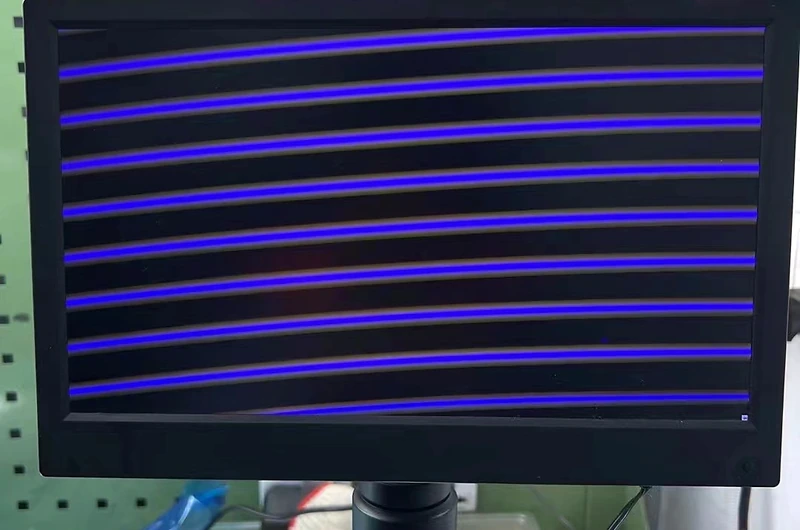
Qualifying an optical mold insert requires objective, non-contact metrology. Visual inspection under fluorescent lighting only reveals whether a surface appears bright, not whether it meets functional optical tolerances.
| Metrology Technology | Measured Metric / Parameter | Primary Functional Purpose | Optical Tooling Application |
| White Light Interferometry (WLI) | $Sa$, $Sq$, 3D Surface Micro-topography | High-resolution vertical mapping (sub-nanometer) without physical contact | Quantifying micro-roughness and diamond scratch profiles across cavity surfaces |
| Laser Fizeau Interferometry | Wavefront Error, Peak-to-Valley ($PV$), $RMS$ Power | Verifying global flatness, sphericity, and macroscopic form accuracy | Full-aperture transmission/reflection evaluation on flat, spherical, or molded lens inserts |
| Stylus Profilometry (with cutoff filters) | $Ra$, $Rq$, $Rz$, Linear Profile Traces | Tracking linear surface roughness across extended physical traverse lengths | Separating low-frequency macro-waviness from high-frequency micro-roughness |
When receiving finished optical tooling, request a comprehensive metrology report documenting measured $Ra$/$Rq$ parameters along with corresponding surface topography plots, rather than a simple visual sign-off sheet.
Sourcing Checklist: How to Evaluate an Optical Polishing Service Provider
Engaging an external vendor for optical cavity finishing requires verifying specialized technical and operational controls. Use this technical checklist when qualifying potential manufacturing partners:
| Sourcing Evaluation Dimension | Critical Engineering Audit Requirement | Supplier Verification Method |
| Abrasive Isolation Protocols | Clear physical separation between rough grinding, intermediate lapping, and fine diamond polishing | Audit clean-room or clean-bench environments to ensure prevention of airborne cross-contamination |
| Substrate Metallurgy Competence | Experience with specified high-performance alloys (ESR tool steels, NAK80, carbide grades) | Confirm processing records that maintain heat-treatment integrity without temper softening |
| In-House Optical Metrology | Availability of non-contact 3D profilometers, WLI, or laser interferometers | Verify calibration certificates and request sample 3D surface map deliverables |
| Edge & Shut-Off Protection | Established fixturing, masking, or sacrificial witness block methodologies | Ensure strict preservation of parting lines and shut-off surfaces to prevent injection flash |
| RFQ Data & Specification Package | Clear 2D/3D documentation detailing optical zones, $Ra$ targets, datums, and removal limits | Review supplier DFM feedback on dimensional allowances and stock removal thresholds |
Reviewing an external partner’s contract optical polishing capabilities upfront prevents downstream tooling delays and costly dimensional adjustments during mold commissioning.
Key Takeaways
- Surface Function Dictates Finishing Method: Optical-grade mold finishing requires precise control of form error, wavefront distortion, and micro-roughness, which cannot be achieved through standard decorative mirror buffing.
- Roughness Requires Precise Specification: Use standardized metrics ($Ra$, $Rq$, SPI Class A-1/A-2/A-3) on engineering drawings rather than non-technical terms like “mirror finish.”
- Lapping and Polishing Serve Distinct Functions: Optical lapping establishes geometry, flatness, and form, while optical polishing refines micro-texture and eliminates sub-surface scratches without eroding edges.
- Steel Quality Directly Limits Surface Quality: Electro-Slag Remelted (ESR) steels with uniform hardness (typically 48–54 HRC) prevent pinholing, inclusion pull-out, and orange peel.
- Verification Demands Non-Contact Metrology: Ensure service providers validate optical surface criteria using calibrated white light or laser interferometry rather than subjective visual checks.
FAQ
Can a damaged optical mold cavity be re-polished without losing dimensional datum points?
Yes, provided the surface damage is within the permissible stock removal tolerance. Re-polishing requires localized micro-lapping followed by staged diamond polishing to preserve the existing datum locations and avoid altering cavity depth. If damage exceeds allowable tolerances, selective micro-welding or re-machining the insert may be required before optical re-finishing.
How does a PVD or DLC coating affect an optically polished mold surface?
Physical Vapor Deposition (PVD) or Diamond-Like Carbon (DLC) coatings accurately replicate the underlying substrate texture. A defect or micro-scratch on the steel will remain visible through the coating. Therefore, the substrate must be polished to the final target SPI or optical specification prior to coating application. The coating thickness (typically 1 to 3 µm) must also be factored into precision mold clearances.
What is the practical difference between SPI A-1 and an optical commercial specification?
SPI A-1 defines a finish achieved with a Grade 3 diamond compound, yielding a typical surface roughness of approximately 0.012 to 0.025 µm $Ra$. While suitable for general transparent covers, precision imaging optics, laser collimators, and micro-fluidic tooling often demand sub-nanometer roughness thresholds and strict wavefront figure tolerances that exceed standard SPI benchmarks.