Precision surface processing often presents an engineering tradeoff: over-specifying a component drives manufacturing costs higher, while under-specifying leads to optical scatter, wavefront distortion, or mechanical failure. The core difference between optical polishing vs. lapping lies in their surface outcome and material removal mechanism. Lapping is an aggressive cutting process designed to establish dimensional thickness, parallelism, and broad surface flatness using abrasive slurry on a rigid plate. Optical polishing is a gentle, finishing process that refines surface roughness ($Ra$) down to sub-nanometer levels and corrects optical surface flatness to fractions of a light wavelength ($\lambda$).
Choosing between these finishing techniques requires evaluating three primary factors: micro-roughness thresholds, interferometric flatness tolerances, and total processing time. While lapping produces a uniform, non-reflective matte finish suitable for mechanical interfaces, optical transmission and precision reflection demand true specular reflectance achieved through dedicated precision optical finishing services.
Process Mechanisms: Mechanical Micro-Fracture vs. Chemical-Mechanical Polishing
The physical interaction between the abrasive media and the workpiece determines the distinction between lapping and polishing.
Lapping: Rolling Abrasive Micro-Fracture
During flat lapping, a workpiece rests against a rotating cast iron or composite plate while bathed in a loose abrasive slurry (typically silicon carbide, aluminum oxide, or boron carbide suspended in oil or water). The abrasive grains roll and slide between the workpiece and the lap plate.
As these hard grains roll, their sharp facets introduce localized mechanical micro-fractures into the substrate surface. This three-body abrasion rapidly shears away high spots, delivering high material removal rates (MRR) and uniform stock reduction. Because the material removal relies on brittle micro-chipping, lapping leaves behind a diffuse, grey matte texture with an underlying layer of sub-surface damage (SSD).
Optical Polishing: Elastic Flow and Chemomechanical Planarization
Optical polishing replaces the rigid plate with a viscoelastic medium—such as pitch or polyurethane synthetic pads—and introduces an ultrafine slurry, most commonly cerium oxide, colloidal silica, or fine diamond suspensions.
Instead of three-body rolling fractures, polishing operates primarily through two-body shear, molecular smoothing, and chemical-mechanical interactions:
- Hydrodynamic Planarization: The soft polishing pad conforms elastically to the global geometry while applying pressure to microscopic peaks.
- Chemical Hydrolysis: In optical glasses and silica substrates, the aqueous chemistry hydrolyzes the outer atomic layers, forming a soft hydrated silica gel.
- Mechanical Shear: The soft chemical layer is continuously stripped away by ultrafine particles without fracturing the underlying crystal or glass matrix.
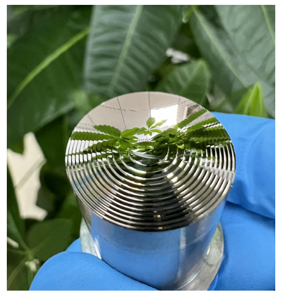
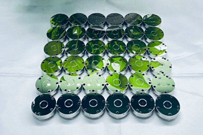
This process removes residual sub-surface micro-cracks from prior grinding steps, resulting in a specular, scatter-free surface that transmits or reflects light without phase distortion.
Flatness vs. Surface Roughness (Ra): Quantitative Tolerance Benchmarks
Engineers frequently confuse flatness with surface roughness. Flatness measures the deviation of an entire surface from a theoretical reference plane (macro-geometry), whereas roughness ($Ra$ or RMS) evaluates high-frequency micro-irregularities across a microscopic sampling length.
Surface Profile and Optical Interaction Comparison
| Process Classification | Surface Topography Profile | Micro-Roughness Range (Ra) | Optical & Functional Behavior | Resulting Surface Appearance |
| Precision Lapping | Micro-fractured, jagged peak-to-valley profile formed by abrasive rolling indentation | Typically $0.1\ \mu\text{m} – 0.8\ \mu\text{m}$ ($100\text{ nm} – 800\text{ nm}$) | Induces high diffuse scattering; prevents specular light transmission; ideal for fluid-retaining mechanical seals | Uniform diffuse grey, non-reflective matte finish |
| Optical Polishing | Planarized, molecularly sheared surface free of sharp micro-peaks and sub-surface fissures | Sub-nanometer to low-nanometer: $0.2\text{ nm} – 2\text{ nm}$ ($<0.002\ \mu\text{m}$) | Near-zero optical scatter; preserves coherent wavefronts; reaches interferometric flatness down to $\lambda/10$ or $\lambda/20$ | Specular, crystal-clear, mirror-like finish |
Quantitative Metrology and Tolerance Differences
| Metric / Parameter | Precision Lapping | Optical Polishing | Standard Verification Metrology |
| Surface Finish ($Ra$) | Typically $0.1\ \mu\text{m} – 0.8\ \mu\text{m}$ ($100\text{ nm} – 800\text{ nm}$) | $0.2\text{ nm} – 2\text{ nm}$ ($<0.002\ \mu\text{m}$) | Contact Profilometer / White Light Interferometer (WLI) |
| Surface Appearance | Matte, diffuse grey, opaque reflection | Specular, mirror-like, crystal clear | Visual / Optical Glossmeter |
| Flatness Tolerance | $1\ \mu\text{m} – 3\ \mu\text{m}$ ($2 – 6$ Helium light bands) | $\lambda/4$ to $\lambda/20$ (e.g., $63.3\text{ nm} – 31.6\text{ nm}$ at $632.8\text{ nm}$) | Laser Fizeau Interferometer |
| Sub-Surface Damage (SSD) | Deep micro-cracks present ($5\ \mu\text{m} – 30\ \mu\text{m}$) | Stripped and eliminated; pristine atomic structure | Cross-sectional SEM / Etch Testing |
| Total Thickness Variation (TTV) | Sub-micron control possible via dual-lap | Maintains or marginally alters pre-existing TTV | Dual-probe capacitance / Micrometer gauge |
| Typical Material Removal Rate | High ($5\ \mu\text{m} – 25\ \mu\text{m}/\text{min}$) | Extremely low ($0.1\ \mu\text{m} – 1.5\ \mu\text{m}/\text{hour}$) | In-situ thickness monitoring |
While double-sided lapping creates excellent dimensional parallelism and planar surfaces across large batches, it cannot reach the sub-nanometer roughness needed for laser optics or imaging windows. Achieving optical clarity requires advanced optical polishing capabilities to smooth micro-peaks and eliminate the crack layer.
Process Cost Drivers: Equipment, Cycle Time, and Yield Economics
The manufacturing cost per piece changes substantially when moving from lapping to optical polishing. Several operational variables govern these cost differences:
1. Cycle Times and Material Removal Rates
Lapping operates at aggressive removal rates, often completing batches in 15 to 45 minutes. Conversely, optical polishing is an inherently slow, controlled process where cycle times often range from several hours to over a full production shift per run. Longer cycles tie up equipment and drive up machine-hour costs.
2. Consumable and Slurry Expenses
- Lapping Media: Standard abrasives (aluminum oxide or silicon carbide) are inexpensive and used in open, high-volume slurry recirculating systems.
- Polishing Media: High-purity, tightly graded optical slurries—such as sub-micron cerium oxide or high-grade polycrystalline diamond—carry higher material costs. Pitch laps also require continuous skilled conditioning and stable temperature environments to maintain their shape.
3. Metrology and Environmental Control
Validating lapped components requires tactile surface profilometers, micrometers, or basic monochromatic light boxes. In contrast, optical polishing verification demands climate-controlled cleanrooms, vibration-isolated optical tables, and phase-shifting laser interferometers to quantify wave error (Peak-to-Valley and RMS). These metrology requirements represent a noticeable capital and labor overhead in final part calculations.
Sequential Finishing: Why Lapping and Polishing Are Often Complementary Steps
Lapping and optical polishing are rarely mutually exclusive in high-precision manufacturing; instead, they serve as consecutive phases in a unified finishing workflow. Attempting to optically polish an as-cut or rough-ground substrate without intermediate lapping results in cycle times that are economically unfeasible and can introduce rolled edges.
| Process Stage | Primary Objectives | Mechanism & Surface State | Key Metrics / Deliverables |
| Raw Substrate | Prepare rough blank for machining | Sawn, wire-cut, or core-drilled blank containing deep saw marks, edge chips, and macro-defects | Rough dimensional envelope; uncalibrated surface finish |
| Coarse & Fine Lapping | Remove bulk stock rapidly; establish thickness and parallelism | Three-body rolling abrasive action micro-fractures high spots, clearing raw saw kerfs and leveling geometry | Target part thickness; sub-micron TTV baseline; uniform diffuse matte finish; introduces uniform sub-surface damage (SSD) |
| Intermediate Pre-Polishing | Eliminate abrasive micro-cracks; transition surface | Soft pads and finer abrasives cut away the residual fractured damage zone without introducing edge roll-off | Strips majority of SSD layer; transitions substrate from diffuse matte to semi-specular; sets stock removal allowance ($15\ \mu\text{m} – 35\ \mu\text{m}$) |
| Precision Optical Polishing | Attain specular clarity and interferometric wave tolerances | Chemical-mechanical planarization (CMP) or pitch finishing relieves surface strain and eliminates micro-peaks | Wavefront error: $\lambda/4$ to $\lambda/20$; surface roughness: $Ra < 1\text{ nm}$; pristine base prepared for dielectric or metallic optical coatings |
Using a unified provider for optical polishing and lapping services protects component quality. The lapping technician leaves a precise stock removal allowance (typically $15\ \mu\text{m}$ to $35\ \mu\text{m}$, depending on the abrasive grain size used) for the polishing stage. This allowance provides enough depth to eliminate all sub-surface fractures while avoiding excessive polishing runs that could degrade edge roll-off or transmitted wavefront performance.
Engineering Decision Framework: When to Stop at Lapping vs. Proceeding to Optical Polishing
To determine whether an engineering drawing requires lapping alone or complete optical polishing, evaluate the functional requirements of the part using the decision matrix below.
Surface Finishing Selection Decision Matrix
| Primary Functional Requirement | Secondary Engineering Condition | Recommended Process | Key Tolerance Capabilities | Typical Component Applications |
| Transmits or Reflects Focused Light | Substrate requires high transmittance, minimal wavefront distortion, or optical thin-film coating | Optical Polishing Required | • Roughness: $Ra < 1\text{ nm} – 2\text{ nm}$ • Flatness: $\lambda/4$ to $\lambda/20$ • Scratch-Dig: 40-20, 20-10, or tighter | Laser windows, optical prisms, mirrors, imaging filters, precision reference flats, sensor viewports |
| Non-Optical / Interface Contact | Requires vacuum/fluid sealing, datum flat registration, or planar conductive heat transfer | Precision Lapping Sufficient | • Roughness: $Ra\ 0.2\ \mu\text{m} – 0.8\ \mu\text{m}$ • Flatness: $1\ \mu\text{m} – 3\ \mu\text{m}$ • TTV: Sub-micron parallelism | Mechanical seal rings, pump valve plates, semiconductor chucks, heat sinks, ceramic spacers |
| Structural / Non-Critical Assembly | Non-sealing, coarse clearance spacing, or general structural support only | Standard Surface Grinding | • Roughness: $Ra > 0.8\ \mu\text{m} – 1.6\ \mu\text{m}$ • Flatness: $10\ \mu\text{m} – 50\ \mu\text{m}$ | Structural base plates, machine brackets, non-critical shim stock, mounting fixtures |
Application Selection Guidance
- Stop at Precision Lapping When:
- The part is a mechanical seal face, valve seat, or ceramic wear plate requiring tight fluid containment under compression.
- The component is a thermal spreader or semiconductor chuck where macro-flatness governs heat transfer, but transparent transmission is unnecessary.
- The primary goal is uniform thickness, tight parallelism (TTV), and dimensional sizing across dense production runs.
- The component serves as a structural datum surface or mounting reference block in machine tooling.
- Specify Full Optical Polishing When:
- The substrate must transmit, refract, or reflect light in lasers, imaging cameras, lithography systems, or spectroscopy setups.
- The part requires optical thin-film coatings (such as anti-reflective, dielectric, or metallic coatings); poor surface finish leads to film peeling and laser-induced damage.
- The design involves viewing windows (fused silica, sapphire, optical glass) where diffuse surface haze impedes sensor clarity.
- The component serves as an optical reference flat, beam splitter, or precision prism where wavefront distortion must stay below $\lambda/4$.
Key Takeaways
- Mechanism: Lapping uses three-body rolling micro-fracture to remove stock quickly; optical polishing applies chemomechanical shear to create a scatter-free surface.
- Surface Metrics: Lapping yields a matte finish with $Ra$ between $0.1\ \mu\text{m}$ and $0.8\ \mu\text{m}$. Optical polishing produces a specular finish with $Ra$ typically below $1\text{ nm}$ to $2\text{ nm}$.
- Flatness Limits: Lapping routinely controls flatness within $1\ \mu\text{m}$ to $3\ \mu\text{m}$. Optical polishing refines surfaces down to sub-micron optical wave fractions ($\lambda/4$ to $\lambda/20$).
- Economics: Lapping features shorter processing times and lower operating overhead. Polishing requires extended cycles, specialized pitch or pad consumables, and interferometric cleanroom metrology.
- Process Flow: These operations are complementary. Lapping sets initial thickness, shape, and parallelism, while polishing eliminates the residual sub-surface micro-fractures left by the abrasive grains.
Frequently Asked Questions (FAQ)
Can lapping alone produce a transparent glass or sapphire surface?
No. Lapping relies on microscopic fracture mechanics that create pits and micro-cracks on the surface. These microscopic irregularities scatter incident light in multiple directions, giving the material an opaque, diffuse matte grey look. Producing an optically transparent surface requires polishing to eliminate those scattering centers.
Does double-sided lapping control parallelism better than single-sided polishing?
Yes. Double-sided planetary lapping finishes both surfaces of a substrate simultaneously between two geared plates. This setup balances cutting forces, minimizes thermal distortion, and delivers tighter total thickness variation (TTV) and parallelism than single-sided mounting techniques, which rely on temporary wax bonding.
What drawing notes indicate that optical polishing is mandatory?
Optical polishing is required when an engineering drawing specifies:
- A surface roughness $Ra \le 0.05\ \mu\text{m}$ ($50\text{ nm}$) or scratch-dig standards (such as MIL-PRF-13830B 60-40, 40-20, or 20-10).
- Flatness tolerances expressed in optical fringe fractions (such as $\lambda/4$, $\lambda/10$, or PV wave error).
- Transmitted Wavefront Error (TWE) or reflected wavefront performance.
Can optical polishing fix poor flatness caused by aggressive lapping?
Only to a limited degree. Polishing removes material at slow rates (often less than $1\ \mu\text{m}$ per hour). Correcting severe taper, thickness variations, or gross curvature during polishing is inefficient and often rounds off the part edges. The pre-polishing lapping stage must establish overall flatness and dimensional limits before final polishing begins.
Technical Consultation and Production Support
Balancing mechanical tolerances and optical requirements prevents unnecessary processing costs during component fabrication. YISHUN evaluates substrate choices, target dimensions, and operating environments to help you choose between flat lapping, pitch polishing, or a combined process flow.
If you are developing custom optical windows, wafers, mirrors, or structural reference flats, our technical team provides manufacturability assessments and process plans based on your drawings. Request an engineering review for optical polishing and lapping services to review technical tolerances, production volumes, and quote specifications.