Selecting the right ultra-precision finishing method depends on whether your component requires sub-aperture figure correction, atomic-level roughness, or complete elimination of sub-surface damage. For optical engineers and sourcing managers evaluating advanced optical polishing services, the choice between Magnetorheological Finishing (MRF), Ion Beam Figuring (IBF), and Chemical Mechanical Planarization (CMP) is rarely a matter of choosing a single “best” technology. Instead, it involves aligning specific surface error signatures, substrate geometries, and laser damage thresholds with the correct removal mechanism.
This technical guide examines how MRF, IBF, and CMP operate, evaluates their performance across key surface metrics, establishes an engineering selection framework, and outlines how multi-stage finishing workflows achieve nanometer-scale tolerances.
The Deterministic Polishing Bottleneck: Beyond Traditional Pitch and Pad Methods
Conventional full-aperture lap polishing and flexible pitch pads have supported precision optical manufacturing for decades. However, these contact-abrasive approaches encounter severe physical boundaries when surface accuracy requirements enter the sub-micron and fractional-wavelength regimes.
Traditional polishing methods exhibit three primary physical constraints:
- Edge Rolloff and Boundary Degradation: Full-aperture laps exert uneven pressure distributions near substrate boundaries, frequently generating edge rolloff that reduces the clear aperture (CA).
- Sub-Surface Damage (SSD): Mechanical grinding and abrasive polishing generate micro-cracks beneath the optical surface. While cosmetic polish may conceal these fractures, latent SSD degrades the Laser-Induced Damage Threshold (LIDT) in high-fluence environments and accelerates coating delamination.
- Limited Deterministic Correction: Conventional laps smooth surfaces across broad spatial frequencies but struggle to address low-frequency surface form errors (Peak-to-Valley wavefront aberrations) without inducing mid-spatial frequency errors (MSFE).
Deterministic sub-aperture finishing resolves these bottlenecks. By delivering a stable, localized, and mathematically characterized material removal footprint, modern advanced finishing enables predictable convergence to targeted wavefront tolerances on complex shapes, including aspherics and freeform optics.
Technical Breakdown: How MRF, IBF, and CMP Remove Material
Understanding when to deploy each advanced technology requires examining how each process removes substrate material at the micro- and nano-scales.
Magnetorheological Finishing (MRF): Shear Force & Magnetic Control
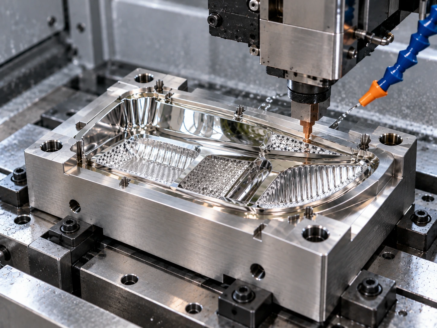
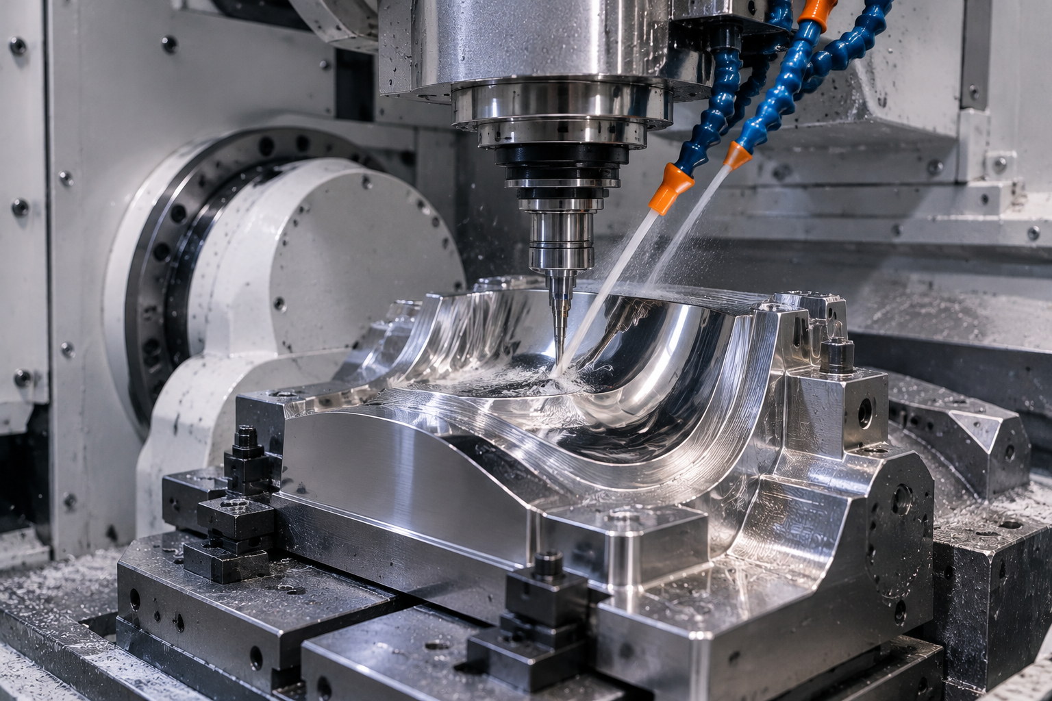
MRF is a sub-aperture polishing method that utilizes a magnetically responsive fluid containing micron-sized magnetic carbonyl iron particles, abrasive particles (such as cerium oxide or diamond), and carrier fluid.
The fluid is pumped onto a rotating wheel. As it passes through an electromagnet, the fluid experiences a local magnetic field, transitioning almost instantly from a Newtonian liquid to an anisotropic quasi-solid plastic ribbon. When the optical workpiece is brought into contact with this stiffened ribbon, material removal occurs entirely via hydrodynamic shear forces rather than direct normal compressive loading. Because the removal tool forms dynamically and continuously refreshes, tool wear is virtually nonexistent, yielding a stable removal function that can correct non-symmetric surface figure errors deterministically.
Ion Beam Figuring (IBF): Non-Contact Atomic Sputtering
IBF is a non-contact, sub-aperture material removal process performed inside a high-vacuum chamber. A directed, neutralized beam of inert gas ions (typically argon) is accelerated toward the target optical surface.
Material removal occurs via physical momentum transfer at the atomic level: incident energetic ions displace substrate atoms through physical sputtering. Because IBF applies zero mechanical force to the workpiece, it introduces no contact stress, zero edge roll-off, and no mechanical micro-fracturing. It operates as a true non-contact trimming tool guided by computer-controlled raster dwell-time algorithms derived directly from interferometric phase maps.
Chemical Mechanical Planarization (CMP): Synergistic Chemical Etch and Abrasion
CMP combines chemical surface softening with ultra-fine abrasive sweeping across a compliant polyurethane pad.
During the CMP process, a chemical slurry reacts with the outermost atomic layers of the substrate to form a delicate, chemically modified passivation layer. Sub-micron abrasive particles suspended in the slurry continuously shear away this softened passivation film from surface peaks, leaving the recessed valleys largely unaffected. This self-limiting planarization mechanism suppresses mechanical subsurface fracturing and planarizes surface topographies down to angstrom-level roughness without generating the directional track marks common to mechanical lapping.
Engineering Comparison: MRF vs. IBF vs. CMP at a Glance
Each technology offers distinct operating envelopes across removal rate, surface roughness (Ra), surface figure accuracy (PV/RMS), and geometric compatibility.
| Engineering Metric | Magnetorheological Finishing (MRF) | Ion Beam Figuring (IBF) | Chemical Mechanical Planarization (CMP) |
| Material Removal Mechanism | Hydrodynamic shear stress via magnetically stiffened abrasive ribbon | Atomic-scale kinetic sputtering via energetic inert gas ion beam | Combined chemical reaction (passivation) and mechanical pad shearing |
| Tool Contact Type | Compliant fluid contact (sub-aperture) | Zero physical contact (vacuum beam) | Compliant contact pad (full or sub-aperture) |
| Primary Engineering Function | Rapid figure error correction & non-symmetric error removal | Final surface figure trimming; stress-free wavefront correction | Atomic planarization; complete removal of sub-surface damage (SSD) |
| Surface Roughness Impact | Typically yields moderate roughness (often $Ra \approx 0.5 – 1.5\text{ nm}$ depending on slurry setup) | Replicates or slightly degrades pre-existing micro-roughness | Consistently achieves ultra-smooth finishes ($Ra < 0.2\text{ nm}$ on compatible glasses) |
| Edge Rolloff Susceptibility | Low to moderate (depends on tool-path velocity control near clear aperture) | Virtually zero (no edge loading or mechanical compliance) | High without dedicated carrier rings or edge-exclusion zones |
| Sub-Surface Damage (SSD) | Low (shear mode minimizes normal load fractures) | Zero induced SSD (removes existing damaged layers atom by atom) | Eliminates existing SSD by planarizing down to the bulk virgin glass |
| Geometry Compatibility | Planar, spherical, high-departure aspheres, and moderate freeforms | Planar, shallow spherical, and moderate aspherical geometries | Primarily flat wafers, prisms, and shallow spherical components |
| Relative Processing Cost / Time | Fast cycle time; moderate equipment and slurry operation cost | Slower removal rate; higher vacuum cycle cost and capital investment | Highly economical for batch flat optics; costly tooling for complex curvatures |
Note: Specific achievable tolerances and surface figures depend on substrate dimensions, glass composition, and machine configuration. Specifications should be confirmed during technical evaluation.
Selection Criteria: Which Polishing Method Suits Your Application?
Determining the appropriate finishing route requires matching functional application demands with process mechanics. The following matrix outlines the primary engineering decision criteria for technology selection.
| Primary Part Condition & Target Specification | Critical Engineering Constraint | Recommended Polishing Technology | Key Advantage |
| Planar or Simple Geometry needing atomic roughness and complete SSD removal | High Laser-Induced Damage Threshold (LIDT) or epi-ready surface requirements | Chemical Mechanical Planarization (CMP) | Clears mechanical fractures and achieves angstrom-scale smoothness via self-limiting chemical etching |
| Complex Aspheric or Freeform Geometry requiring deterministic wavefront correction | Need for rapid figure error convergence and high volumetric removal rates | Magnetorheological Finishing (MRF) | Conformal fluid ribbon avoids tool-mismatch errors and rapidly reduces PV wavefront aberrations |
| Ultra-Thin, Lightweight, or High Clear-Aperture Optics needing final figure trimming | Susceptible to mechanical clamping distortion, back-structure print-through, or edge roll-off | Ion Beam Figuring (IBF) | Zero contact force, stress-free atomic sputtering, and uniform figure correction up to $98\%+$ clear aperture |
When to Select MRF: Fast Convergence for Complex Aspherics & Freeforms
MRF is optimal when an optical component requires rapid, deterministic correction of mid-to-low spatial wavefront errors on non-standard geometries.
- High-Departure Aspheric & Freeform Optics: Because the MRF fluid ribbon conforms to local surface curvature without hard tool mismatch, it handles steep aspherical departures and off-axis geometries that would gouge rigid laps.
- Rapid Convergence of Form Errors: For optics emerging from grinding or rough diamond turning, MRF converges surface figure errors (PV and RMS) significantly faster than full-aperture iteration.
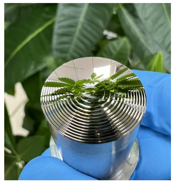
- Mitigating Mid-Spatial Grooving: MRF is frequently selected to buff out diamond-turning tool marks and diffractive rings without altering the underlying macro-geometry.
When to Select IBF: Final Figure Trimming and Stress-Free Optics
IBF is preferred when contact mechanics, mechanical clamping, or edge boundary dynamics pose quality risks.
- Ultra-Thin Mirrors and Lightweight Structures: Lightweight honeycombed mirrors (such as beryllium or silicon carbide space optics) flex under any physical polishing pressure. Because IBF exerts no mechanical force, it corrects surface figures without structural deformation or “print-through” of backing ribs.
- Edge-to-Edge Clear Apertures ($>95\%$ CA): Because no physical pad overhangs or rounds the part boundary, IBF figure correction can be applied up to the extreme peripheral edges of optical mirrors.
- Final Sub-Nanometer Figure Trimming: When an optical wavefront must reach fractional sub-aperture tolerances ($\lambda/20$ to $\lambda/100$ or better), IBF performs predictable, atomic-scale material removal without tool-wear variations.
When to Select CMP: Super-Smooth Surfaces & Zero Sub-Surface Damage
CMP is the preferred process when surface roughness and chemical purity govern performance rather than complex aspheric figuring.
- High-Power Laser Substrates: Optics subjected to high-energy pulsed laser systems require high Laser-Induced Damage Thresholds. CMP gently etches away fractured subsurface layers left behind by mechanical abrasives, preventing thermal absorption sites.
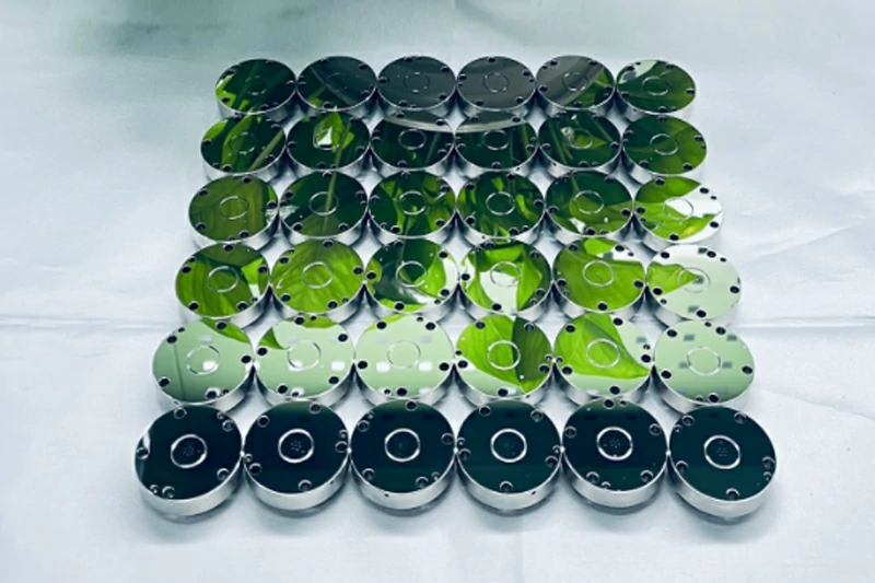
- Semiconductor Substrates and Optical Flats: Silicon, fused silica, sapphire, and quartz substrates for lithography and wafer-level optics demand planar surfaces with angstrom-level microroughness across entire batches.
- Epi-Ready Crystal Wafers: Materials such as GaN, SiC, and single-crystal quartz require CMP to yield defect-free atomic step surfaces suitable for downstream dielectric or epitaxial thin-film coating.
Complementary Synergy: Building a Multi-Stage Finishing Chain
High-end optical systems rarely depend on a single processing technique. Advanced precision optical polishing and lapping services integrate these methods into a complementary multi-stage chain:
| Sequence Stage | Manufacturing Operation | Primary Objective & Function | Typical Target Metric |
| Stage 1: Pre-shaping & Damage Removal | Conventional Pitch Lapping / CMP | Removes deep micro-cracks from rough grinding; establishes clean baseline geometry | Baseline roughness $Ra < 1.0\text{ nm}$; elimination of brittle subsurface fractures |
| Stage 2: Deterministic Figure Correction | Magnetorheological Finishing (MRF) | Rapidly corrects low- and mid-frequency wavefront figure errors across aspheric/freeform zones | PV reduction to $\le \lambda/4$ or target aspheric sag profile within minimal iterations |
| Stage 3: Non-Contact Final Figure Trimming | Ion Beam Figuring (IBF) | Conducts atomic-scale sputtering to trim residual errors and eliminate tooling edge effects | Wavefront uniformity down to $\lambda/20 – \lambda/100$; stress-free finish across full aperture |
| Stage 4: Metrology Verification & Quality Gate | Multi-Angle Interferometry & Profilometry | Validates 100% clear-aperture phase maps, residual roughness, and compliance with LIDT limits | Full-aperture surface figure report, PSD power spectrum, and $Ra$ verification data |
This hybrid sequence leverages the high volumetric removal speed of MRF, the atomic surface smoothing of CMP, and the stress-free non-contact accuracy of IBF.
RFQ Checklist: What to Prepare Before Requesting Optical Polishing Quotes
To ensure an accurate engineering review and quotation from an optical manufacturer, provide the following parameters in your drawing package:
- Material Specification: Clear identification of the substrate (e.g., Corning 7980 Fused Silica, CVD Silicon Carbide, N-BK7, Zerodur, Germanium) and any pre-existing thermal treatments or dopant concentrations.
- Surface Figure / Wavefront Accuracy: State the required Peak-to-Valley (PV), Root-Mean-Square (RMS), or wavefront error tolerances explicitly (e.g., $\lambda/10$ PV at $632.8\text{ nm}$ over clear aperture).
- Surface Microroughness ($Ra$ / $Rq$): Distinguish between cosmetic surface quality (MIL-PRF-13830B or ISO 10110 scratch-dig) and quantitative profilometry roughness ($Ra$ in angstroms or nanometers).
- Clear Aperture (CA) Boundaries: Define the required active optical area. If the aperture extends past $95\%$ of the physical diameter, highlight this requirement so the manufacturing team can configure edge-safe toolpaths (such as IBF).
- Sub-Surface Damage & LIDT Specifications: For high-power laser applications, explicitly state required laser operating parameters (wavelength, pulse duration, repetition rate) and subsurface damage thresholds to determine whether chemical planarization passes are mandatory.
- CAD Models & Departure Data: For aspherical or freeform components, provide the sag equation, polynomial coefficients, and 3D step files to support machine kinematic modeling.
Key Takeaways
- MRF excels at rapid, deterministic figure correction on complex aspheric and freeform surfaces via controlled shear forces, making it the most cost-effective solution for wavefront error convergence.
- IBF is a non-contact, vacuum-based atomic sputtering technique designed for final figure trimming, edge-to-edge clear apertures, and ultra-thin, stress-sensitive optical mirrors.
- CMP provides atomic-level surface smoothing and complete removal of subsurface damage through synergistic chemical etching and mechanical polishing, which is critical for maximizing Laser-Induced Damage Thresholds.
- Hybrid Workflows combining preliminary CMP smoothing, deterministic MRF figuring, and final IBF non-contact trimming provide the highest-performing manufacturing route for mission-critical optics.
Frequently Asked Questions (FAQ)
Can MRF completely eliminate mid-spatial frequency errors (MSFE)?
MRF significantly reduces mid-spatial frequency errors when programmed with optimized raster toolpaths and appropriate sub-aperture ribbon widths. However, because MRF uses a finite-sized removal footprint, improper step-over spacing can occasionally leave subtle directional signatures (ripple). In ultra-critical applications, components receive a final smoothing run or non-contact IBF pass to disperse residual MSFE.
Why is IBF not used for all optical material removal?
IBF operates through atomic-scale sputtering, which results in a low volumetric material removal rate compared to fluid or abrasive polishing. Removing tens of microns of material with an ion beam is economically impractical and time-prohibitive. Consequently, IBF is reserved strictly as a final correction step after mechanical or fluid polishing has brought the optical surface within fractions of a wavelength of the target figure.
Which optical materials are compatible with Chemical Mechanical Planarization (CMP)?
CMP is compatible with a wide range of single-crystal, poly-crystal, and amorphous optical materials, including fused silica, optical glasses, silicon, sapphire, gallium arsenide (GaAs), and silicon carbide (SiC). The chemical formulation of the slurry (acidic vs. alkaline) and the abrasive chemistry (silica, alumina, or ceria) must be tailored specifically to the substrate material to achieve the necessary passivation balance.
How does sub-surface damage affect Laser-Induced Damage Threshold (LIDT)?
Sub-surface damage consists of microscopic fractures, micro-cracks, and embedded polishing particles residing directly beneath an apparently polished surface. Under high-fluence laser irradiation, these subsurface defects act as focal points that trap electromagnetic energy, initiating thermal absorption, localized plasma formation, and catastrophic surface failure. Employing CMP or deep-etch finishing removes this defective layer, substantially raising the component’s LIDT.