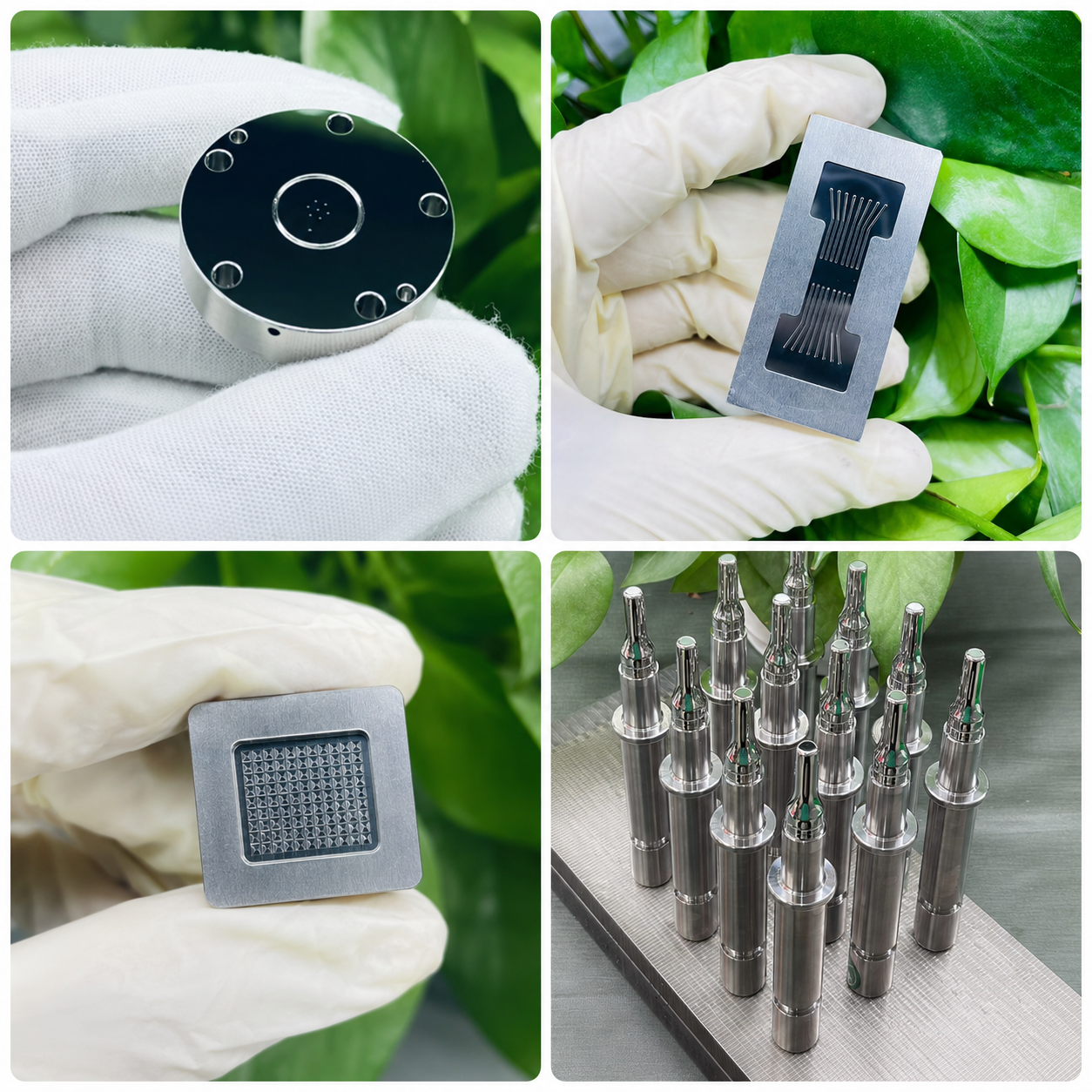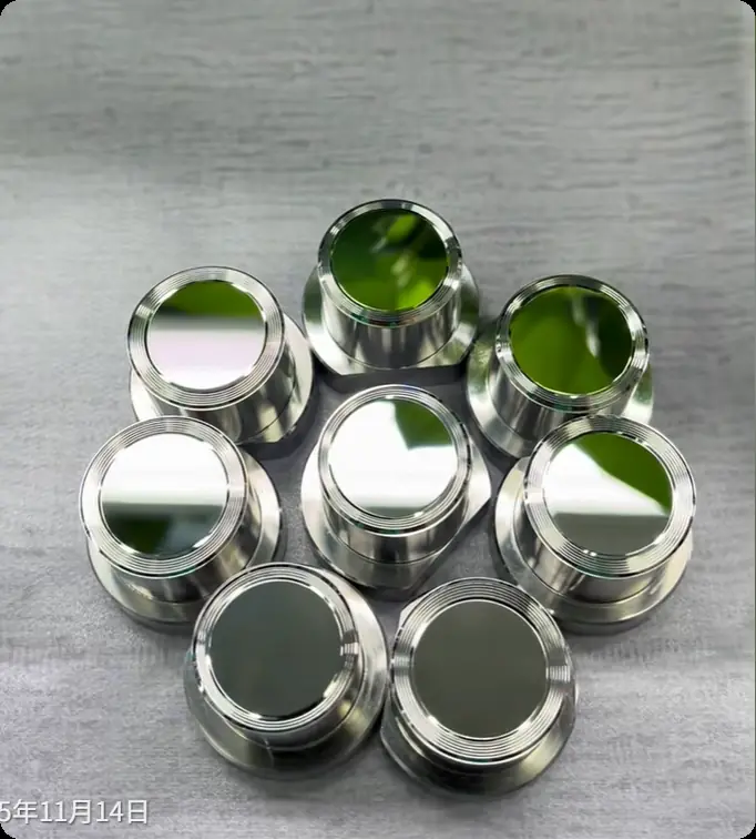
Optical lapping services are used to improve the flatness, parallelism, thickness uniformity, and surface condition of precision optical components before final polishing, coating, bonding, or assembly. For components such as optical windows, glass substrates, quartz plates, sapphire parts, ceramic parts, wafers, and precision sealing surfaces, lapping is often a critical process for achieving stable geometry and reliable performance.
Unlike general surface finishing, precision optical lapping focuses on controlled material removal. The goal is not only to make a surface smoother, but also to make the component dimensionally accurate, flat, stable, and suitable for its final optical or mechanical function.
For B2B projects involving high-precision optical parts, choosing the right optical polishing and lapping services provider can help reduce problems such as poor contact, uneven thickness, optical distortion, bonding failure, and assembly misalignment.
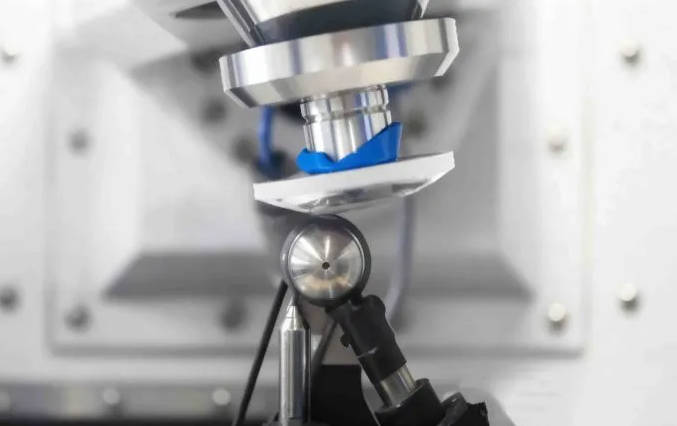
What Are Optical Lapping Services?
Optical lapping is a precision abrasive machining process used to remove small amounts of material from a component surface. During lapping, the workpiece is moved against a lapping plate with abrasive slurry or fixed abrasive media. This controlled action gradually improves the surface geometry and prepares the part for final polishing or functional use.
The main purpose of optical lapping is to control geometry, especially flatness, parallelism, and thickness, before the component moves to polishing, coating, or assembly.
Optical lapping services are commonly used for:
- Optical windows
- Glass plates and substrates
- Quartz and fused silica components
- Sapphire components
- Ceramic components
- Silicon wafers and substrates
- Precision spacers
- Sealing surfaces
- Optical filters
- Laser and photonics components
- Semiconductor-related parts
- Precision mechanical and optical assemblies
In many applications, lapping is performed before optical polishing. Lapping controls the shape and thickness of the part, while polishing improves the final surface roughness and optical clarity.
Why Flatness and Parallelism Matter in Optical Components
Flatness and parallelism are not just drawing requirements. They directly affect how a component performs in an optical system, mechanical assembly, or precision instrument.
Flatness describes how much a surface deviates from a perfect plane. Parallelism describes how evenly two opposite surfaces align with each other. When either parameter is poorly controlled, the finished part may create optical distortion, alignment errors, uneven bonding, poor sealing, or mechanical instability.
For optical windows, substrates, wafers, and precision plates, flatness and parallelism can be as important as surface roughness because they affect both optical path stability and mechanical fit.
For example:
| Requirement | Why It Matters |
|---|---|
| Flatness control | Helps maintain optical alignment, bonding quality, sealing contact, and stable assembly |
| Parallelism control | Reduces wedge error and supports consistent optical path or mechanical spacing |
| Thickness uniformity | Helps parts fit into assemblies and maintain predictable optical or mechanical behavior |
| Surface consistency | Reduces local high spots, pressure points, and irregular contact |
| Edge stability | Reduces chipping risk during handling, mounting, and assembly |
In optical and photonics applications, even a small wedge or uneven surface can affect beam direction, image quality, or assembly repeatability. In mechanical and semiconductor-related applications, poor flatness may lead to poor contact, uneven pressure, or unreliable bonding.
Optical Lapping vs. Grinding vs. Polishing
Lapping is often confused with grinding and polishing. Although these processes are related, each one has a different purpose in the production chain.
| Process | Main Purpose | Surface Result | Geometry Control | Typical Use |
|---|---|---|---|---|
| Grinding | Shape the part and remove larger amounts of material | Rough or semi-finished surface | Moderate | Pre-forming, thickness reduction, shape preparation |
| Lapping | Improve flatness, parallelism, and thickness uniformity | Fine matte or semi-polished surface | High | Flat optical parts, substrates, wafers, plates |
| Polishing | Improve surface roughness, clarity, and optical quality | Smooth, transparent, reflective, or optical-grade surface | Depends on process | Lenses, windows, mirrors, final optical surfaces |
Grinding shapes the component, lapping controls the geometry, and polishing refines the final surface quality. In many high-precision projects, all three processes may be used in sequence.
For customers who need both surface geometry control and optical finishing, Yishun Optical provides precision optical lapping and polishing services for custom components used in optical, industrial, and technical applications.
How the Precision Optical Lapping Process Works
The exact lapping process depends on material, part size, geometry, thickness, and tolerance requirements. However, a typical optical lapping workflow includes several key stages.
1. Drawing and Specification Review
The supplier first reviews the customer’s drawing, material, quantity, dimensional tolerances, surface requirements, flatness, parallelism, and application. This step is important because lapping requirements must be measurable and realistic.
Key questions include:
- What material is being processed?
- What is the required final thickness?
- Is one-side or double-side lapping needed?
- What flatness is required?
- What parallelism is required?
- Will the part be polished after lapping?
- Will the surface be coated, bonded, sealed, or assembled?
- What inspection method is required?
If the drawing only says “high precision” or “good flatness,” the supplier may need further clarification before quoting.
2. Pre-Processing or Cutting
The raw material may need to be cut, machined, sliced, or ground before lapping. This prepares the part close to the final size and removes large material allowances.
For brittle materials such as glass, quartz, sapphire, and ceramics, this step must be controlled carefully to reduce edge chips, cracks, or subsurface damage.
3. Rough Lapping
Rough lapping removes remaining material and begins improving flatness and thickness uniformity. Larger abrasive particles may be used at this stage, depending on the material and removal requirement.
The goal is to bring the part closer to the required geometry while maintaining process stability.
4. Fine Lapping
Fine lapping uses finer abrasives and more controlled conditions to further improve flatness, parallelism, and surface consistency. This step is important before optical polishing or final inspection.
The supplier may adjust pressure, speed, slurry, plate condition, and cycle time to control the final result.
5. Cleaning
After lapping, parts must be cleaned to remove abrasive particles, slurry residue, and surface contamination. Poor cleaning can cause scratches during later polishing or handling.
6. Inspection
The finished or semi-finished part is inspected for flatness, thickness, parallelism, surface condition, and dimensional accuracy. Inspection methods depend on part requirements and customer specifications.
7. Optional Polishing
If the part requires optical transparency, low roughness, or final optical surface quality, polishing may follow lapping. For many optical windows, filters, mirrors, and substrates, lapping and polishing are used together.
Key Tolerances in Optical Lapping Services
Different projects require different tolerances. A small optical window, a large glass substrate, a sapphire plate, and a ceramic sealing component may all require different process strategies.
The most common tolerance parameters include:
| Tolerance Parameter | Meaning | Why It Matters |
|---|---|---|
| Flatness | Deviation from a perfect plane | Affects contact, bonding, sealing, and optical path stability |
| Parallelism | Relationship between two opposite surfaces | Reduces wedge error and supports consistent spacing |
| Thickness tolerance | Allowed final thickness variation | Important for assembly fit and optical path control |
| Surface roughness | Microscopic surface texture | Affects polishing readiness, sealing, and surface function |
| Dimensional tolerance | Final length, width, diameter, or shape accuracy | Ensures part fits into the final assembly |
| Edge quality | Condition of edges after lapping | Reduces risk of chips, cracks, and handling damage |
| Surface defect control | Scratches, pits, chips, stains, or embedded particles | Affects downstream polishing, coating, and performance |
The most important specifications for precision optical lapping are usually flatness, parallelism, thickness tolerance, and surface condition.
In many cases, customers should avoid specifying unnecessarily tight tolerances unless the application truly requires them. Excessively strict flatness or parallelism requirements can increase cost, production time, inspection complexity, and yield risk.
Single-Sided Lapping vs. Double-Sided Lapping
Depending on the component and tolerance requirements, suppliers may use single-sided or double-sided lapping.
| Item | Single-Sided Lapping | Double-Sided Lapping |
|---|---|---|
| Process Method | One surface is processed at a time | Both sides are processed simultaneously |
| Main Advantage | Flexible for complex or one-sided requirements | Better for thickness uniformity and parallelism |
| Common Use | Parts requiring one controlled surface | Plates, wafers, substrates, spacers, windows |
| Parallelism Control | Possible, but may require multiple setups | Generally more suitable for two-sided parallelism |
| Part Suitability | Useful for non-symmetric parts | Useful for flat components with two functional faces |
| Typical Limitation | More setup-dependent | May be less suitable for some irregular shapes |
For optical windows, wafers, plates, and substrates, double-sided lapping is often considered when both flatness and parallelism are important. Single-sided lapping may be more suitable when only one functional surface needs precise control or when part geometry does not allow double-sided processing.
Materials Commonly Used in Precision Optical Lapping
Material behavior strongly affects lapping strategy. Hardness, brittleness, thermal expansion, internal stress, and chemical resistance all influence process selection.
| Material | Lapping Considerations |
|---|---|
| Optical glass | Requires careful control of scratches, edge chips, and flatness |
| Quartz | Often used for optical, thermal, and chemical resistance applications |
| Fused silica | Requires clean processing and stable surface preparation |
| Sapphire | Very hard and wear-resistant, but more difficult to process |
| Silicon | Often requires tight flatness and thickness control |
| Ceramics | Brittle and prone to chipping without proper process control |
| Optical crystals | May require material-specific handling and orientation awareness |
| Metal mirror substrates | May need controlled surface preparation before polishing or coating |
For hard and brittle materials, the lapping process must balance removal rate, surface damage, and edge protection. Aggressive removal may save time but can introduce chips, cracks, or subsurface damage.
Factors That Affect Flatness and Parallelism Control
Precision lapping is a controlled process, but the final result depends on many variables.
Material Stability
Materials with internal stress or uneven structure may deform during processing. Thin parts are especially sensitive to stress release and handling pressure.
Part Thickness and Size
Large, thin, or fragile components are more difficult to keep flat. They may bend during processing, cleaning, inspection, or mounting.
Lapping Plate Condition
The condition of the lapping plate affects flatness consistency. Plate wear, surface condition, and maintenance are important process factors.
Abrasive Selection
Abrasive type and particle size affect removal rate, surface finish, and subsurface damage. Coarser abrasives remove material faster, while finer abrasives improve surface condition.
Process Pressure
Too much pressure can deform fragile parts or cause uneven removal. Too little pressure may reduce efficiency or create inconsistent results.
Carrier and Fixturing
Fixtures, carriers, and part positioning influence how evenly the surface is processed. Improper support may cause non-uniform thickness or wedge.
Cleaning and Handling
Particles left on the surface can create scratches. Poor handling may create edge chips or surface contamination after lapping.
Inspection Method
Flatness and parallelism must be measured using appropriate inspection tools. If the inspection method is not agreed upon, supplier and customer may have different interpretations of the result.
Common Applications of Optical Lapping Services
Precision optical lapping is used in many industries where flatness, thickness, and surface geometry affect product performance.
Optical Windows and Plates
Optical windows often require controlled flatness and parallelism to maintain light transmission and reduce beam deviation. Lapping prepares the surfaces before final polishing or coating.
Glass and Quartz Substrates
Substrates used in optical, semiconductor, and scientific equipment may require uniform thickness and stable flatness for bonding, coating, or assembly.
Sapphire Components
Sapphire is used in applications that require hardness, wear resistance, transparency, or chemical stability. Lapping is often needed to control thickness and surface geometry before polishing.
Semiconductor and Wafer-Related Components
Lapping can be used for wafers, carriers, spacers, and other precision components that require flat surfaces and controlled thickness.
Laser and Photonics Components
Laser and photonics systems often require stable optical paths. Lapped and polished surfaces can help support alignment, transmission, and assembly reliability.
Precision Sealing and Contact Surfaces
In some mechanical or vacuum-related applications, lapped flat surfaces help improve contact, sealing, or load distribution.
Common Mistakes When Buying Optical Lapping Services
Many lapping project issues come from unclear communication or incomplete technical requirements.
| Mistake | Potential Issue | Better Approach |
|---|---|---|
| Asking only for “high flatness” | Supplier cannot quote or inspect accurately | Define flatness requirement and inspection method |
| Ignoring parallelism | Finished part may have wedge or uneven spacing | Specify parallelism if both sides are functional |
| Not providing final thickness | Process allowance may be incorrect | Provide starting and final thickness requirements |
| Over-tightening tolerance | Higher cost and longer lead time | Match tolerance to functional need |
| Not discussing material risks | Chips, cracks, or low yield may occur | Confirm material-specific processing experience |
| Forgetting edge requirements | Parts may chip during handling or assembly | Specify chamfer, bevel, or edge protection |
| Not confirming polishing needs | Lapped surface may not meet optical clarity needs | Clarify whether polishing is required after lapping |
A clear RFQ for optical lapping should include material, drawing, dimensions, thickness, flatness, parallelism, surface condition, edge requirements, quantity, and application.
How to Choose an Optical Lapping Services Supplier
Selecting a supplier for precision lapping requires more than comparing price. The process depends on technical experience, equipment stability, inspection capability, and communication quality.
1. Material Experience
Confirm whether the supplier has experience with your material. Lapping glass is different from lapping sapphire, ceramics, silicon, or fused silica.
2. Flatness and Parallelism Capability
Ask whether the supplier can support your required flatness and parallelism level for the specific part size and material. Capability should be discussed based on your actual drawing, not only general claims.
3. Combined Lapping and Polishing Capability
Many optical components require both lapping and polishing. A supplier with both capabilities can better manage process continuity and reduce coordination risk.
Yishun Optical offers optical lapping and polishing services for precision components that require geometry control and finished optical surfaces.
4. Inspection Support
The supplier should be able to inspect the parameters that matter to your project, such as flatness, thickness, parallelism, surface roughness, and visual defects.
5. Engineering Communication
A qualified supplier should review your drawing, identify unclear specifications, and suggest practical manufacturing options. This is especially important for prototype and custom optical parts.
6. Handling and Packaging
Finished lapped and polished surfaces can be sensitive to scratches, chips, and contamination. Proper handling and packaging help protect the parts before assembly or further processing.
For companies evaluating custom optical finishing partners, Yishun Optical provides optical processing support for components used in industrial, optical, photonics, and technical applications.
What Information Should You Provide for a Lapping RFQ?
To receive a practical quotation, provide as much technical information as possible.
| RFQ Item | Why It Matters |
|---|---|
| Material | Determines abrasive, process speed, and risk control |
| Drawing or CAD file | Defines dimensions, geometry, and tolerance requirements |
| Starting thickness | Helps estimate material removal allowance |
| Final thickness | Required for process planning and inspection |
| Flatness requirement | Defines the main geometry target |
| Parallelism requirement | Important for double-sided functional parts |
| Surface roughness target | Determines whether fine lapping or polishing is needed |
| Edge requirement | Helps prevent chipping and handling damage |
| Quantity | Affects pricing, setup, and production planning |
| Application | Helps supplier understand functional priorities |
| Inspection requirement | Defines acceptance standard and reporting needs |
If you are not sure how to specify flatness or parallelism, describe the final application first. A supplier can then help recommend a realistic and cost-effective requirement.
Conclusion
Precision optical lapping services are essential for components that require controlled flatness, parallelism, thickness uniformity, and reliable surface preparation. Lapping is widely used for optical windows, glass substrates, quartz plates, sapphire components, wafers, ceramics, photonics parts, semiconductor-related components, and precision sealing surfaces.
For B2B buyers, the most important step is to define the required geometry and inspection criteria clearly. Material, part size, thickness, flatness, parallelism, surface condition, edge quality, and downstream polishing requirements all affect the final process plan.
If your project requires flatness lapping, parallelism control, or combined polishing and lapping for custom optical components, Yishun Optical can support your project through precision optical polishing and lapping services from technical review to finished component delivery.
FAQ
What are optical lapping services used for?
Optical lapping services are used to improve flatness, parallelism, thickness uniformity, and surface consistency of optical components. They are commonly used for glass plates, optical windows, quartz parts, sapphire components, wafers, substrates, and precision sealing surfaces.
What is the difference between optical lapping and optical polishing?
Optical lapping mainly controls geometry, including flatness, parallelism, and thickness. Optical polishing mainly improves the final surface roughness, clarity, and optical quality. Many precision optical components require both processes.
Why is flatness important in precision optical lapping?
Flatness is important because it affects optical alignment, bonding quality, sealing contact, and assembly stability. Poor flatness can cause uneven contact, optical distortion, or mechanical fit problems.
How does lapping control parallelism in optical components?
Parallelism is controlled by removing material evenly from one or both sides of the component. Double-sided lapping is commonly used when two opposite surfaces must maintain consistent spacing and reduced wedge.
What materials can be processed by precision lapping services?
Common materials include optical glass, quartz, fused silica, sapphire, silicon, ceramics, optical crystals, and some metal substrates. Each material requires a suitable abrasive, process pressure, and handling method.
Do lapped optical parts always need polishing afterward?
Not always. Some parts only require flatness, thickness control, or sealing contact, so lapping may be sufficient. If the part requires optical transparency, low roughness, or final optical surface quality, polishing is usually needed after lapping.
What should I include in an RFQ for optical lapping services?
A complete RFQ should include material, drawing, dimensions, starting thickness, final thickness, flatness, parallelism, surface roughness, edge requirements, quantity, application, and inspection criteria.